ウェーハレベル・オプティクス(WLO)
Market-leading WLO manufacturing portfolio, including step-and-repeat mastering, lens molding, nanoimprint lithography and stacking
Introduction
EVG's wafer-level optics (WLO) manufacturing solutions enable a multitude of novel optical sensing devices for mobile consumer electronics products. Key examples include 3D sensing, biometric authentication, environmental sensing, infrared sensing and microlens arrays. Other applications include automotive front-lights, light carpets, optical diffusers and medical imaging.
EVG's WLO solutions are supported by the company's NILPhotonics Competence Center.
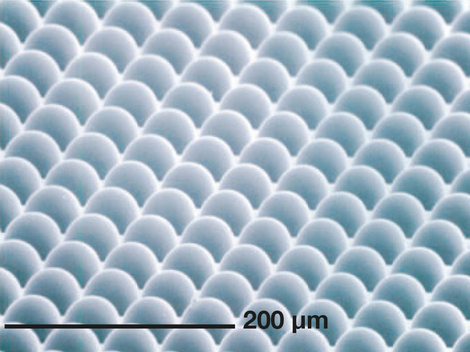
Step-and-Repeat Mastering
Master stamps are wafer-size templates fully populated with microlens molds, each replicated from a single lens or lens array template in a step-and-repeat (S&R) approach. Starting from a single lens master made out of metal, silicon or glass, EV Group offers all essential process steps for the fabrication of master stamps featuring unmatched lens position accuracies and lens shape repeatability.
Find out more about the EVG®770 NT Step-and-Repeat Nanoimprint Lithography System
UV Microlens Molding
Lens patterns are transferred into optical polymer materials by soft UV imprint lithography using working stamps replicated from the wafer-size master stamps. EV Group offers hybrid and monolithic microlens molding processes, which can be easily adapted to various material combinations for working stamp and microlens materials. EVG systems are our customers’ first choice for high-volume wafer-level lens replication.
Find out more about the EVG®7300 Multifunctional UV Nanoimprint Lithography System
SmartNIL®
EVG provides market-leading UV-nanoimprinting equipment with its robust and field-proven SmartNIL technology. Progress in photonic manufacturing processes and technologies as well as applications is closely linked to advances in equipment capabilities. Among these, recent developments in SmartNIL offer additional degrees of freedom to manufacture innovative photonic structures with the highest functionality and smallest form factors at high volumes. With this technology, diffractive optical elements (DOEs) and optical waveguides can be easily integrated into miniaturized optical modules.
Find out more about our SmartNIL® technology
Lens Stacking
The final micro optics stack is fabricated by UV bonding of all elements, including individual double-side microlens wafers as well as spacer wafers, to achieve the final stack height. Crucial parameters are lens-to-lens alignment accuracy, total thickness variation and tilt of the resulting bond interface.
Find out more about the IQ Aligner® Automated UV Nanoimprint Lithography System
Features
- Efficient step-and-repeat master fabrication
- Volume-proven imprinting technology with superior replication fidelity
- Precision aligned lens molding and stacking
- Proprietary SmartNIL® technology
- Multiple-use polymer stamp technology
- Open materials platform


Related products

Talk to our EVG technology experts!
Questions?

Questions about our technologies?
Contact the EVG experts
EVG in the Press
Europhotonics featured our article "Wafer-Level Optics Enables Small-Form Photonics Sensors" in its 2020 spring edition