検査・計測
Process control and optimization for lithography and bonding
Introduction
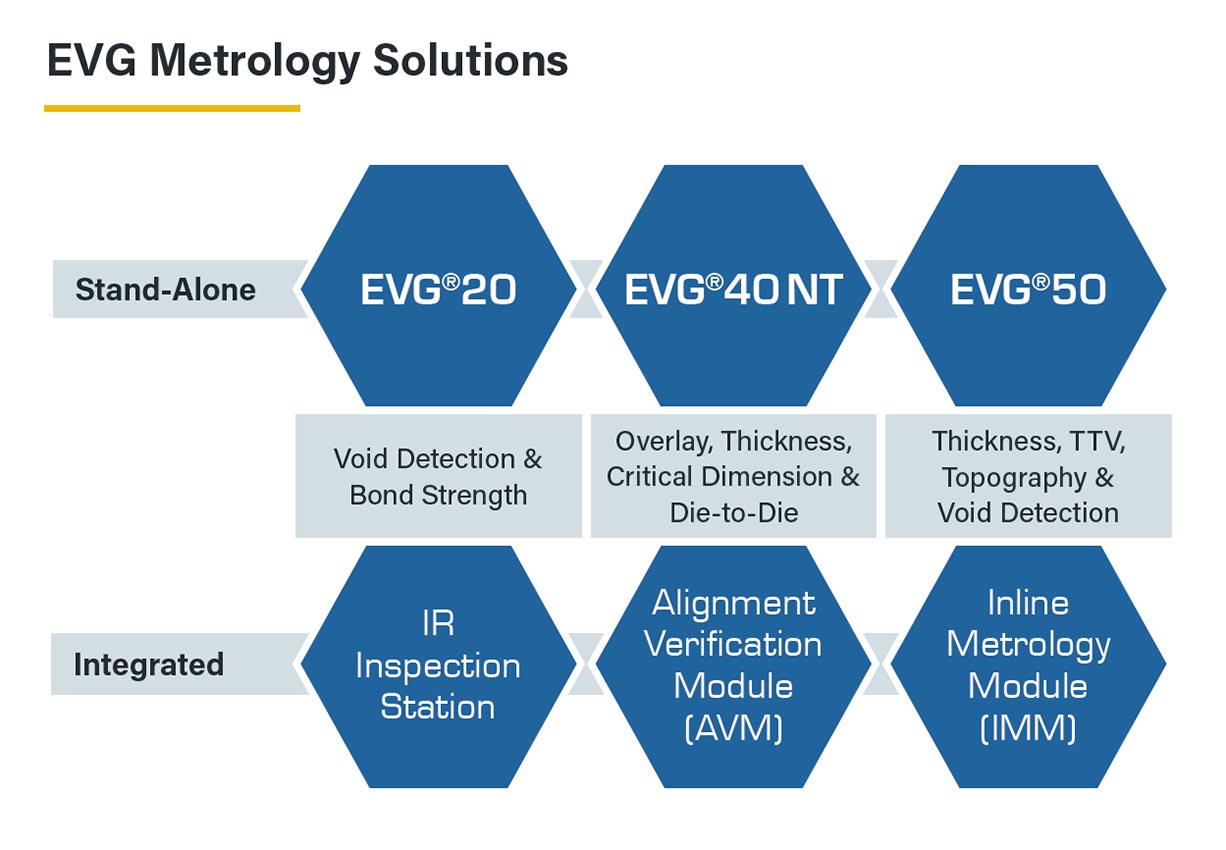
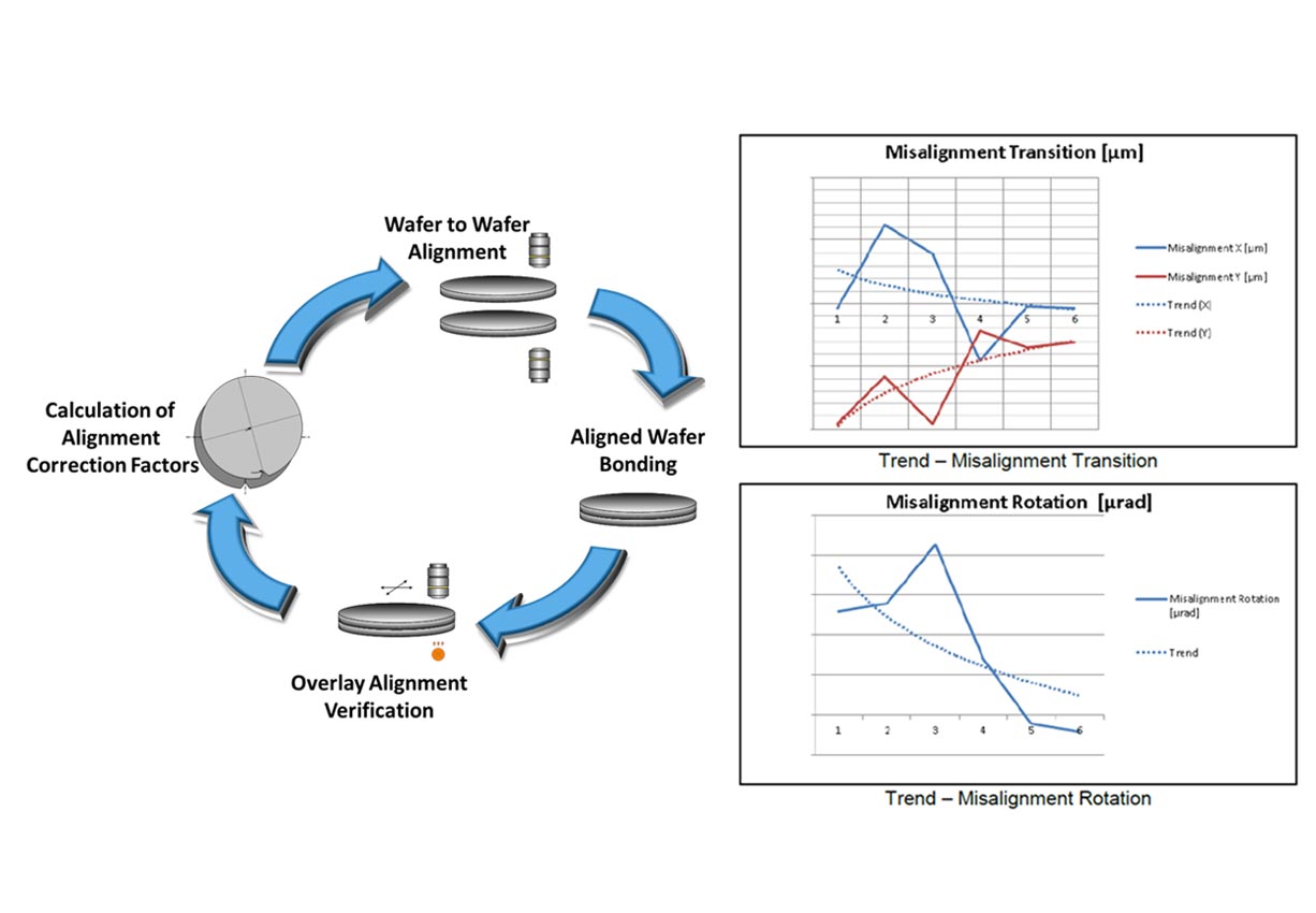
To complete EVG’s lithography and bonding portfolio, sufficient metrology is necessary to ensure process control and (in combination with feedback loops) also allow for process parameter optimization like bond alignment. Versatile measurement options are available to meet the metrology requirements for a wide variety of applications. These tools can fit in HVM and R&D environments.
Metrology is essential to control, optimize and ensure the highest yield in semiconductor manufacturing processes. Advanced packaging, MEMS and photonic applications are gaining importance, very often lacking suitable metrology solutions for essential processing steps. Furthermore, overall performance of the device is determined by packaging and back-end-of-line processes; hence, process requirements are getting tighter and need further metrology. EVG’s metrology solutions for wafer inspection and evaluation are optimized for lithography and all types of bonding applications. As one example, metrology prior to non-reworkable processes like wafer thinning after temporary bonding directly leads to increased yield and process security, where an integrated feedback loop results in a reduction of high-cost wafer scrap.
Features
- Adaptiveness
- Multi-sensor measurement mount for highest metrology flexibility
- Sensor set available for multiple measurement ranges and materials
- Self-calibration of measurement units for minimum service and maintenance
- Integration in stand-alone or production tool
- Handling
- Handling and metrology of various substrates materials, shapes, stress, bow or warp
- Bridge capability for different substrate sizes and carrier mounted wafers
- Available with multiple load port options and combinations
- Control
- Feedback loop for correction of process parameters
- Customized Pass/Fail criteria for automated processing decisions
- Fully integrated SECS/GEM interface
Related products

Talk to our EVG technology experts!
Questions?
Events
Semicon South East Asia 2026
Visit our booth #1126 and listen to our talk “Advanced Lithography Technologies for Packaging: Enabling Next Gen Plasma Dicing Applications” at the Techstage on 06th of May held by Deputy Process Technology Manager Europe Tobias Zenger.

9th International Workshop on Low Temperature Bonding for 3D Integration LTB-3D 2026
Listen to our talk “Xenon vs Argon Ion Activation for Room‑Temperature Wafer Bonding of Si and SiC” held by Senior Process Technology Engineer Peter Kerepesi.
More information here.

ITF World 2026
Visit our booth at ITF World 2026!
Questions about our technologies?
Contact the EVG experts

