スピン塗布
平面のコーティングに適したスピン塗布技術
イントロダクション
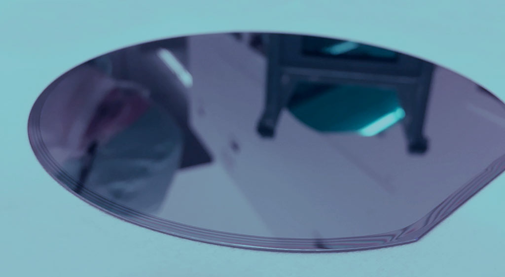
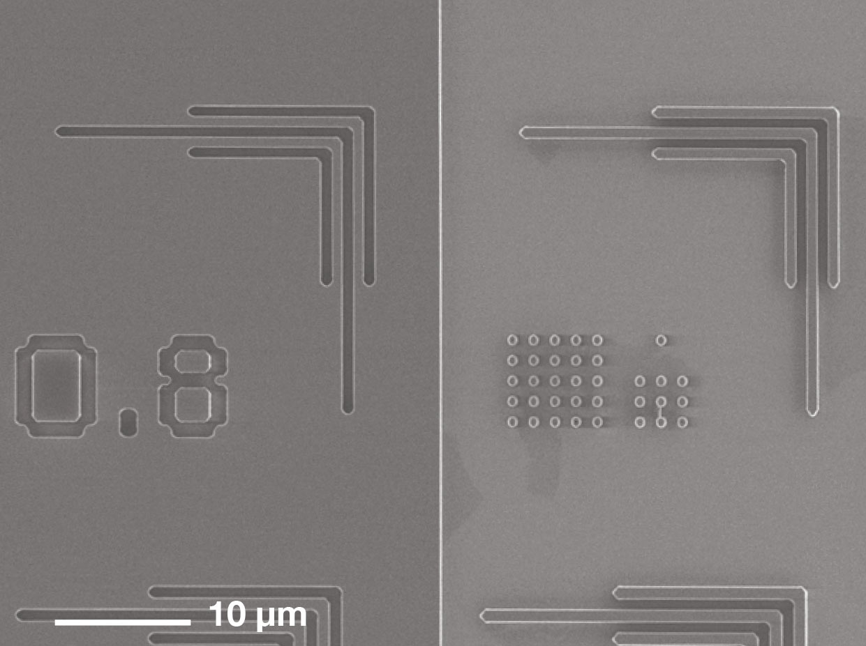
スピン塗布技術は、段差構造のないウェーハ上に、均一な薄膜を塗布するための普遍的かつ集中的に用いられるプロセスです。
Related technologies
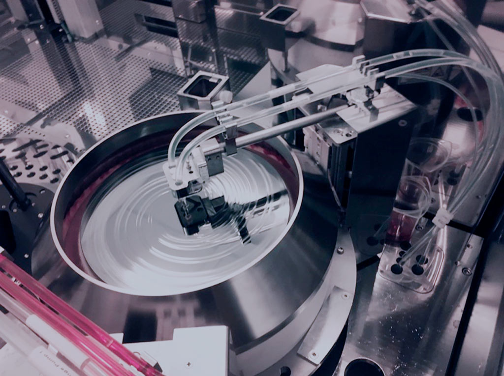
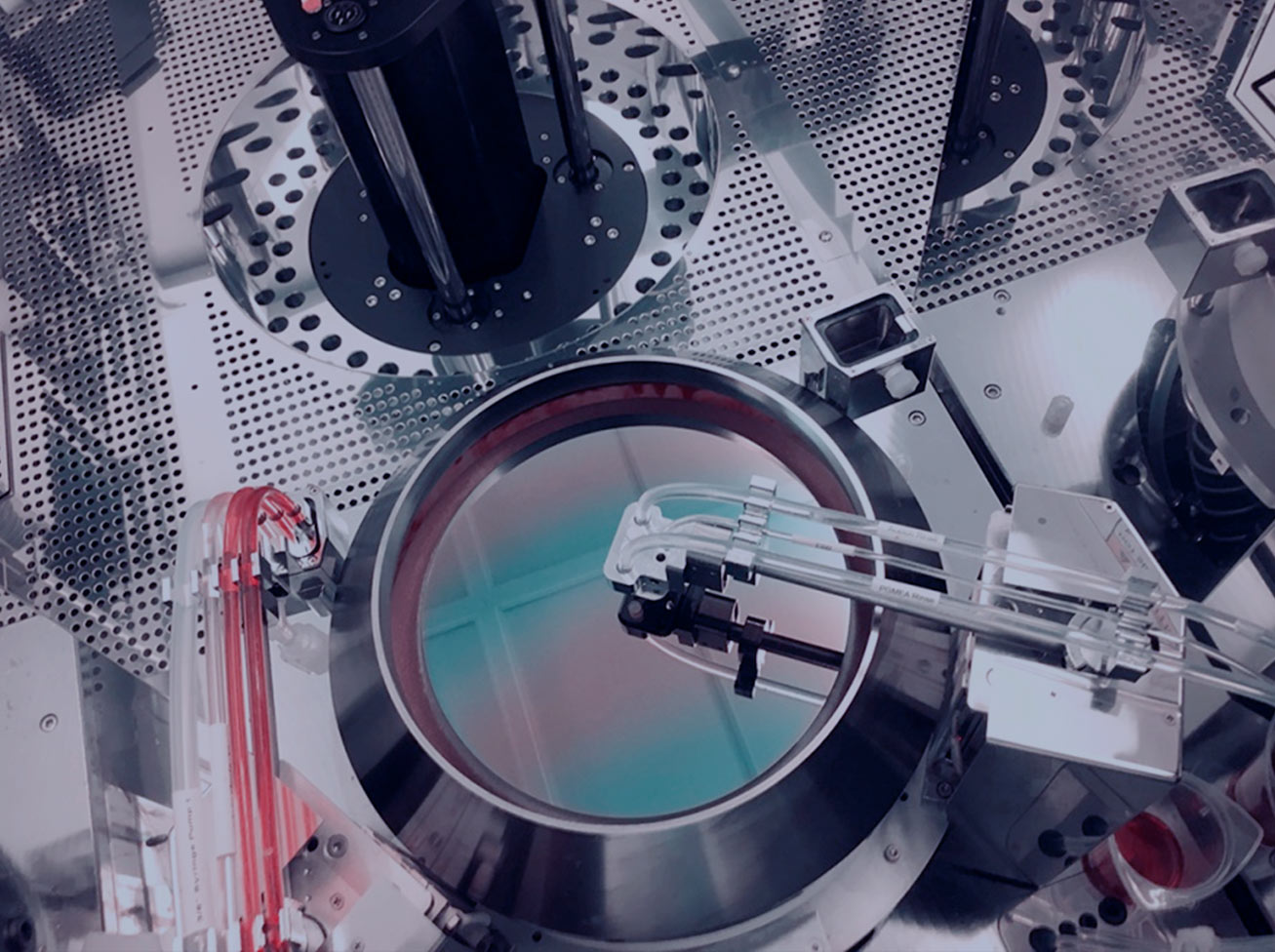
塗布材料の正確なディスペンスと、スピン速度の精密な制御は、スピン塗布プロセスにおいて最も重要な要素となります。基板の回転および加速度、緻密なスイベルアームと基板の位置決め、または動的なディスペンス量の精度など、その他のプロセスパラメータも、塗布工程において重要な役割を果たします。EVGのスピン塗布装置は、これらの重要なパラメータをすべて制御し、正確なレジスト塗布のプロセス制御が行えるように設計されています。ディスペンスラインは温度制御なしで最大8本、または温度制御付きで最大4本まで搭載可能で、3種類の異なるディスペンス方式をサポートするプロセス設定により、最大52.000 cPまでの幅広い粘度のレジストに対して最適な結果を保証します。静的または動的センター・ディスペンス・モードは、一般的な薄膜アプリケーションや標準的な粘度のレジストを使用する際に推奨されます。エリア・ディスペンス・モードにより、均一性とレジスト消費量を最適化し、BCBやSU-8などの高粘度レジスト使用時に極めて均一な厚さのレジスト層を形成することができます。さらに、エッジ・ディスペンス・モードは、エッチング保護を目的とした典型的なアプリケーションとなり、特に長時間のエッチングプロセスにおいて用いられます。この目的のために、EVGの装置には、基板の各種フラット/ノッチ規格をサポートするプログラム可能なスイベルアームが装備されています。また、溶剤によるプリウエット、エッジビード除去、自動溶剤補充可能な密閉型スイベルアーム・パークポジションなどの追加機能により、高度なプロセス制御と量産使用における各種要件に対応します。プログラム可能なサックバック機能により、ノズル先端から基板表面への余分なレジスト滴下を防ぎ、基板全面をコンフォーマルな状態に保ちます。オプションのCoverSpinにより、基板1枚あたりの塗布材料の使用量を削減し、基板形状に依存せずに、エッジ部分で生じる気流の乱れによるプロセス結果への影響を回避することができます。EVGのスピンコートモジュールは、シミュレーションに基づく低乱流設計により、塗布材料を効率的に使用しながら平面や低段差構造において高い均一性を実現できるように設計されています。
特長
- 精密なレシピで制御されたレジスト塗布プロセス
- 最大52000cPの粘度のフォトレジストに対応する3種類のディスペンス・モード
- シミュレーションに基づくコートモジュール形状の低乱流設計
- 各種フラット/ノッチ規格に対応するプログラム可能なスイベルアーム
- 溶剤によるプリウエットやエッジビード除去などの機能を追加し、高度なプロセス制御を実現
- 自動溶剤補充可能な密閉型スイベルアーム・パークポジション
- プログラム可能なサックバック機能
- CoverSpin™技術により、基板形状に依存しないコーティング膜の均一性向上と、乱気流によって発生するエッジ効果の排除
- スマートなプロセス制御とデータ解析ソフトウェア機能
- プロセスおよび機械制御のための統合された解析機能
- 並列タスク/キューイングタスク処理機能
- 装置やプロセスのパフォーマンス・トラッキング機能
- スマートハンドリング機能
- 発報・アラーム解析
- スマートな保守管理・トラッキング
Talk to our EVG technology experts!
Questions?
Events
SEMICON Europa 2026
Visit our booth #B1241 at SEMICON EUROPA 2026 & our poster presentations at the APC:
“Software-Driven Strategies for Advanced Multi-Die Patterning in Digital Lithography “ presented by Business Development Manager Dr. Ksenija Varga and ”Leveraging Advanced Bonding Technologies to Enable Scalable Co-Packaged Optics Architectures” introduced by Business Development Manager Elisabeth Brandl.
Here you'll find more Information on the program.
Furthermore you'll find our Corporate Sales & Marketing Director Thomas Uhrmann at the Panel Discussion “SEMICONDUCTOR TOUR 2026” presented by YOLE Group on 12th of November at the Novotel München Messe. Click here for more Information.
Industrial Print Integration Conference (IPI) 2026
Listen to our Keynote “Advancing AR/VR and CPO: EV Group’s Inkjet Solutions for Next-Generation Optics” held byJohanna Rimböck (Technology Development).
For more information about the program click here.
EPTC 2026
Visit our Booth #2 & listen to our talks:
"Scalable Manufacturing Approaches for Co-Packaged Optics via NIL and Advanced Wafer Bonding" held by Director Business Development Dr. Bernd Dielacher.
“Advancing 310×310 mm² Panel Level Packaging: High Throughput Pathways to High Yield 3D Integration” and “Plasma–Enabled Die Singulation on Film Frame Carrier for Advanced HBM and Logic Die Integration” by Business Development Manager Dr. Ksenija Varga.
“Hybrid Bonding Overlay Reduction Through Lithographic Pre-Compensation of the Residual Fingerprint” by Technical Program Manager Sander Grosemans.
EVG & Brewer Science: “Polymer Buffer Layer Enabling a Novel RDL–First Process Flow using a Silicon Carrier and IR Laser Debonding Technology” shared presentation, Peter Urban & Brewer Science.
EVG & CEA–Leti: “Nanometer Level Chip- Scale Transfer Enabled by IR Laser Debond Technology”.
Check out the program here.
Questions about our technologies?
Contact the EVG experts