EN
English (EN)
Menu
- Products
-
Technologies
- IR LayerRelease™ Technology
- MLE™ - Maskless Exposure Technology
- Nanoimprint Lithography (NIL) - SmartNIL®
- Wafer Level Optics
- Optical Lithography
- Resist Processing Technology
- Temporary Bonding and Debonding
- Eutectic Bonding
- Transient Liquid Phase (TLP) Bonding
- Anodic Bonding
- Metal Diffusion Bonding
- Hybrid and Fusion Bonding
- Die-to-Wafer Fusion and Hybrid Bonding
- ComBond® Technology
- Metrology
- Company
- Careers
Search
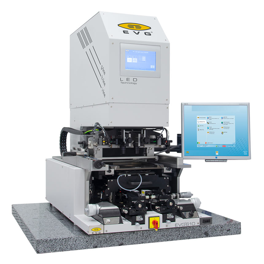
EVG®610
UV Nanoimprint Lithography System
Mask alignment system with UV Nanoimprint Lithography capability from small pieces up to 150 mm
The tool supports a variety of standard lithography processes, such as vacuum-, soft-, hard- and proximity exposure mode, with the option of back-side alignment. In addition, the system offers conventional UV Nanoimprint Lithography (soft UV-NIL) and allows quick processing and re-tooling for changing user requirements with a conversion time between lithography and NIL of just a few minutes. Its advanced multi-user concept can be adapted from beginners to expert level, thus making it ideal for universities and R&D applications.
Features
- Top-side and bottom-side alignment capability
- High-precision alignment stage
- Automated wedge error compensation mechanism
- Motorized and recipe-controlled exposure gap
- Supports the latest UV-LED technology
- Minimized system footprint and facility requirements
- Step-by-step process guidance
- Remote tech support
- Multi-user concept (unlimited number of user accounts and recipes, assignable access rights, different user interface languages)
- Agile processing and conversion between lithography processes
- Table top or stand-alone version with anti-vibration granite table
- Additional capabilities:
- Bond alignment
- IR alignment
- Nanoimprint lithography
- µ-contact printing
Technical Data
| Wafer diameter (substrate size) |
|---|
| Standard lithography: pieces up to 150 mm |
| Soft UV-NIL: pieces up to 150 mm |
| Resolution |
|---|
| ≤ 40 nm (resolution dependent upon template and process) |
| Supported Process |
|---|
| Soft UV-NIL |
| Exposure source |
|---|
| Mercury light source or UV LED light source |
| Automated separation |
|---|
| Not supported |
| Working stamp fabrication |
|---|
| External |
Related downloads

Talk to our EVG product experts!
Questions?
Related technologies
Questions about our products and technologies?
Contact the EVG experts
Related News
