- Products
-
Technologies
- IR LayerRelease™ Technology
- MLE™ - Maskless Exposure Technology
- Nanoimprint Lithography (NIL) - SmartNIL®
- Wafer Level Optics
- Optical Lithography
- Resist Processing Technology
- Temporary Bonding and Debonding
- Eutectic Bonding
- Transient Liquid Phase (TLP) Bonding
- Anodic Bonding
- Metal Diffusion Bonding
- Hybrid and Fusion Bonding
- Die-to-Wafer Fusion and Hybrid Bonding
- ComBond® Technology
- Metrology
- Company
- Careers
Events
Semicon South East Asia 2026
Visit our booth #1126 and listen to our talk “Advanced Lithography Technologies for Packaging: Enabling Next Gen Plasma Dicing Applications” at the Techstage on 06th of May held by Deputy Process Technology Manager Europe Tobias Zenger.

9th International Workshop on Low Temperature Bonding for 3D Integration LTB-3D 2026
Listen to our talk “Xenon vs Argon Ion Activation for Room‑Temperature Wafer Bonding of Si and SiC” held by Senior Process Technology Engineer Peter Kerepesi.
More information here.

ITF World 2026
Visit our booth at ITF World 2026!

ECTC 2026
Visit our booth #220 and visit our PDC "Wafer-to-Wafer and Die-to-Wafer Hybrid Bonding for Heterogeneous Integration and Advanced Packaging" on Tue, May, 26 and listen as well to our talk “Digital Lithography Patterning of Novel Dry Film Resists for High Aspect Ratio Cu Pillar Applications on 310x310mm2 Panel Substrates” held by Business Development Manager Dr. Ksenija Varga on 29th of May.
Here you'll find more information on the program.

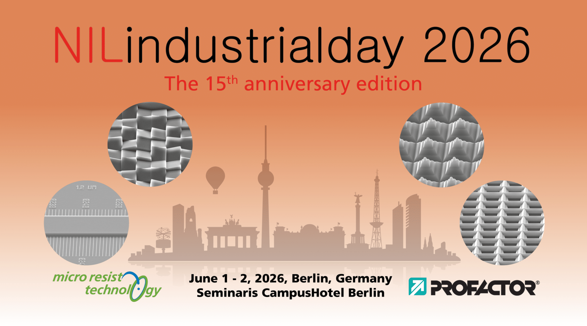
NIL Industrial Day 2026
Visit our Booth and listen to our talk "Scaling Photonic Packaging: The Role of UV Nanoimprint Lithography” held by Senior Process Technology Engineer Patrick Schuster.
For more information follow the link.

Leti Innovation Days 2026
Visit us at our booth at the Leti Innovation Days 2026!