- Products
-
Technologies
- IR LayerRelease™ Technology
- MLE™ - Maskless Exposure Technology
- Nanoimprint Lithography (NIL) - SmartNIL®
- Wafer Level Optics
- Optical Lithography
- Resist Processing Technology
- Temporary Bonding and Debonding
- Eutectic Bonding
- Transient Liquid Phase (TLP) Bonding
- Anodic Bonding
- Metal Diffusion Bonding
- Hybrid and Fusion Bonding
- Die-to-Wafer Fusion and Hybrid Bonding
- ComBond® Technology
- Metrology
- Company
- Careers
Transient Liquid Phase (TLP) Bonding
Low-temperature metal wafer bonding by Transient Liquid Phase (TLP)
Introduction
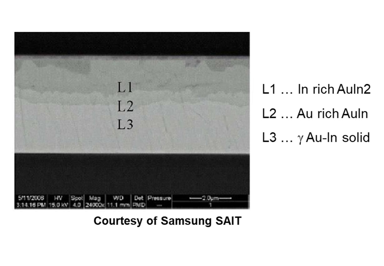
Transient Liquid Phase (TLP) bonding is often used when high-reliability bond lines or electric connections are needed. In this process, the interlayer melts, and the interlayer element diffuses into the substrate materials, thereby causing isothermal solidification. This results in a bond that has a higher melting point than the bonding temperature.
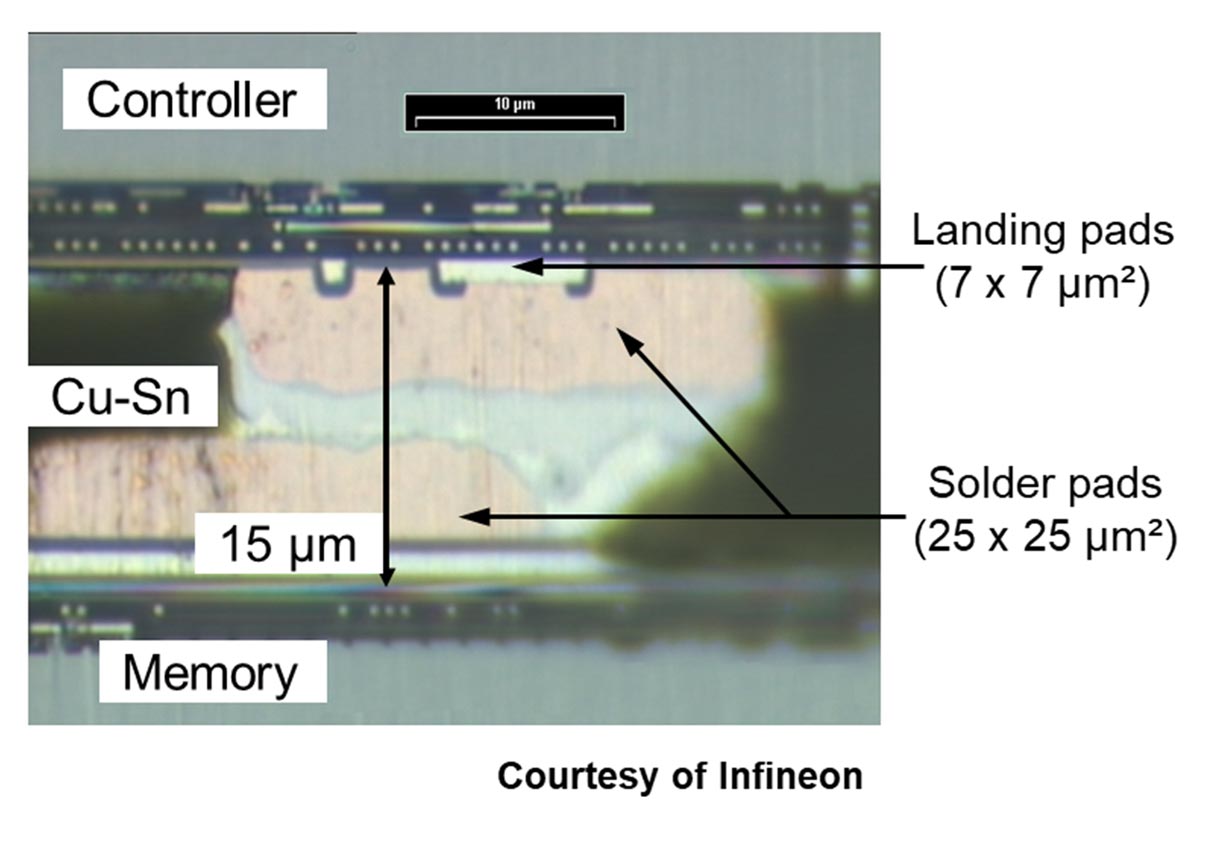
The unique characteristic feature of Transient liquid phase (TLP) bonding is that the liquid bond interface solidifies by diffusion but not by cooling below a melting point compared to eutectic bonding. This enables low process temperatures while providing much higher remelt temperature after joining the wafers. In particular, the interlayer is a low melting point material that moves into the lattice and grain boundaries of the high melting point parent materials, thereby forming an inter-metallic layer. In TLP, it is important to select a suitable interlayer based on the flow characteristics, stability and wettability in order to form a composition that provides faster diffusion characteristics and high reliability. Compared to other bonding technologies, TLP is an advanced type of solder bonding method that can form hermetic sealing at lower temperatures. It is ideal for MEMS vacuum packaging, as the process can be performed at low temperatures compatible with CMOS standards and the resulting bonded devices can withstand harsh environments with high temperatures.
Features
- Vacuum encapsulation
- Defined pressure encapsulation
- Conductive process
- Hermetic sealing
- Good mechanical strength
- Low temperature process
- Less applied force during bonding
- Very good post-bond alignment
- Applied in many metallic and ceramic systems
- Joints with uniform composition profile

Talk to our EVG technology experts!
Questions?
Events
Semicon South East Asia 2026
Visit our booth #1126 and listen to our talk “Advanced Lithography Technologies for Packaging: Enabling Next Gen Plasma Dicing Applications” at the Techstage on 06th of May held by Deputy Process Technology Manager Europe Tobias Zenger.

9th International Workshop on Low Temperature Bonding for 3D Integration LTB-3D 2026
Listen to our talk “Xenon vs Argon Ion Activation for Room‑Temperature Wafer Bonding of Si and SiC” held by Senior Process Technology Engineer Peter Kerepesi.
More information here.

ITF World 2026
Visit our booth at ITF World 2026!
- IR LayerRelease™ Technology
- MLE™ - Maskless Exposure Technology
- Nanoimprint Lithography (NIL) - SmartNIL®
- Wafer Level Optics
- Optical Lithography
- Resist Processing Technology
- Temporary Bonding and Debonding
- Eutectic Bonding
- Transient Liquid Phase (TLP) Bonding
- Anodic Bonding
- Metal Diffusion Bonding
- Hybrid and Fusion Bonding
- Die-to-Wafer Fusion and Hybrid Bonding
- ComBond® Technology
- Metrology
Questions about our technologies?
Contact the EVG experts

