- Products
-
Technologies
- IR LayerRelease™ Technology
- MLE™ - Maskless Exposure Technology
- Nanoimprint Lithography (NIL) - SmartNIL®
- Wafer Level Optics
- Optical Lithography
- Resist Processing Technology
- Temporary Bonding and Debonding
- Eutectic Bonding
- Transient Liquid Phase (TLP) Bonding
- Anodic Bonding
- Metal Diffusion Bonding
- Hybrid and Fusion Bonding
- Die-to-Wafer Fusion and Hybrid Bonding
- ComBond® Technology
- Metrology
- Company
- Careers
MLE™ Maskless Exposure Technology
Moving beyond traditional mask-based lithography toward digital lithography technology
Introduction
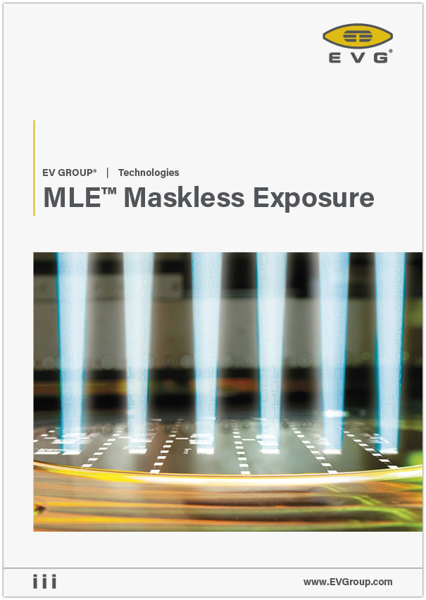
MLE (maskless exposure) technology is a revolutionary next-generation lithography technology developed by EV Group to address future back-end lithography needs for advanced packaging, MEMS, biomedical and IC substrate applications. The world’s first highly scalable maskless lithography technology for high-volume manufacturing delivers unsurpassed flexibility to enable extremely short development cycles for new devices.
Heterogeneous integration is gaining more attention and is seen as a forthcoming way of achieving higher computing performances and extended device functionalities without the need for continuous scaling. The demand for the continuous innovation of the chiplet design and its integration on silicon or on package can be addressed via adaptive patterning. This new industry vision will require new high-volume manufacturing tools that can quickly integrate new designs schemes as traditional back-end lithography suffers from several limitations restricting its applicability. Moreover, continuously increasing mask costs for various layout designs and mask inventory management represents a significant part of overall development and production costs. MLE technology invented by EV Group addresses this critical demand for design flexibility, as it surmounts mask-related difficulties in both development and production phases and thus shortens development cycles. Additionally, this technology keeps your specific designs and layouts confidential as they do not need to be sent externally. This innovative ‘digital lithography’ technology bridges the gap between R&D and production while offering a scalable solution capable of dynamically addressing die and wafer-level designs simultaneously and at the same time meet critical requirements for various markets, such as advanced packaging, MEMS, biomedical and HDI PCB markets.
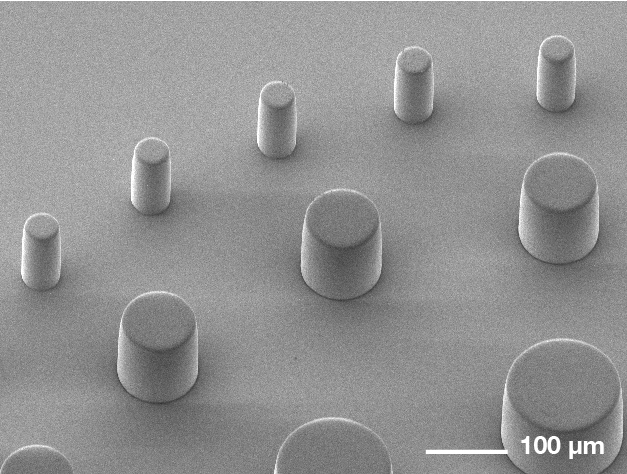
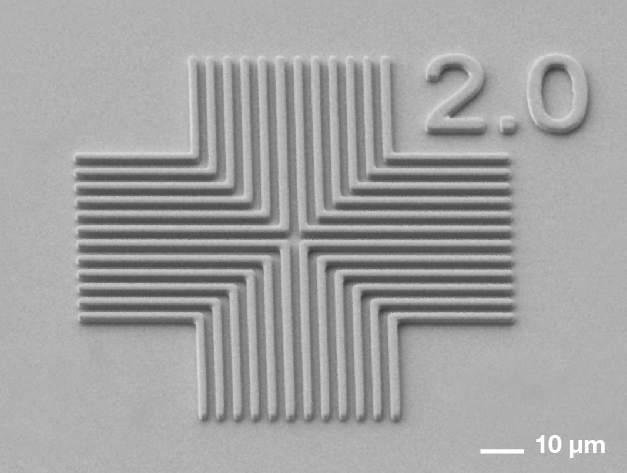
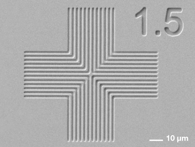
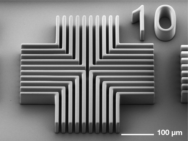
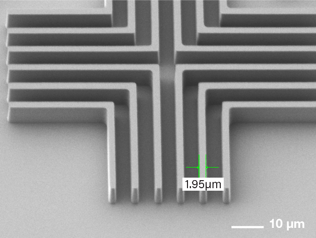
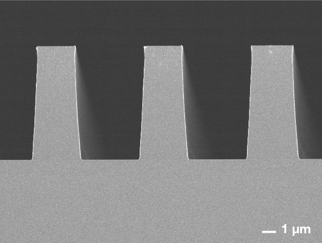
EVG’s MLE technology enables high-resolution (<2 microns L/S), stitch-free maskless exposure of the entire substrate surface with high throughput and low cost of ownership. The system scales according to user needs – for facilitating rapid transition from R&D to HVM mode, for throughput optimization, or for adaptation to different substrate sizes and materials – and is ideal for processing a range of substrates from small silicon or compound semiconductor wafers up to panel sizes. MLE achieves the same patterning performance regardless of photoresist thanks to a flexible and scalable high-power UV laser source, which provides multiple wavelength exposure options.
The aim of EVG’s novel MLE technology is not only to bring a new lithography tool to the market, but also address a critical need for smart and agile digital processing in the semiconductor industry while delivering unique maskless scalability in throughput, format and consumables-free infrastructure
Features
- Full-resolution, stitch-free dynamic photoresist patterning
- Better than 2 µm line / space resolution in any arbitrary direction
- Design freedom and data confidentiality thanks to digital programmable layouts
- Individual die annotations (serial numbers, encryption keys, etc.)
- Compensation of wafer level adaptive registration
- Unaffected by substrate deformation and warpage (thick wafers, glass, or organic substrates)
- Smart & agile digital lithography processing infrastructure
- Consumables-free technology
Figures
Related downloads
Related products

Talk to our EVG technology experts!
Questions?
Events
Semicon South East Asia 2026
Visit our booth #1126 and listen to our talk “Advanced Lithography Technologies for Packaging: Enabling Next Gen Plasma Dicing Applications” at the Techstage on 06th of May held by Deputy Process Technology Manager Europe Tobias Zenger.

9th International Workshop on Low Temperature Bonding for 3D Integration LTB-3D 2026
Listen to our talk “Xenon vs Argon Ion Activation for Room‑Temperature Wafer Bonding of Si and SiC” held by Senior Process Technology Engineer Peter Kerepesi.
More information here.

ITF World 2026
Visit our booth at ITF World 2026!
Share this page with your colleagues on LinkedIn
- IR LayerRelease™ Technology
- MLE™ - Maskless Exposure Technology
- Nanoimprint Lithography (NIL) - SmartNIL®
- Wafer Level Optics
- Optical Lithography
- Resist Processing Technology
- Temporary Bonding and Debonding
- Eutectic Bonding
- Transient Liquid Phase (TLP) Bonding
- Anodic Bonding
- Metal Diffusion Bonding
- Hybrid and Fusion Bonding
- Die-to-Wafer Fusion and Hybrid Bonding
- ComBond® Technology
- Metrology
Questions about our technologies?
Contact the EVG experts
