- Produkte
-
Technologien
- IR LayerRelease™ Technology
- MLE™ - Maskless Exposure Technologie
- Nanopräge-Lithographie (NIL) - SmartNIL®
- Wafer-Level Optics
- Optische Lithographie
- Fotolackverarbeitung
- Temporäres Bonden und De-Bonden
- Eutektisches Bonden
- Transient Liquid Phase (TLP) Bonden
- Anodisches Bonden
- Metall-Diffusionsbonden
- Hybrid- und Fusionsbonden
- Die-to-Wafer Fusion and Hybrid Bonding
- ComBond® Technologie
- Metrologie
- Unternehmen
- Karriere
HERCULES® NIL
Fully Integrated SmartNIL® UV-NIL Systems
EVG's HERCULES® NIL product family
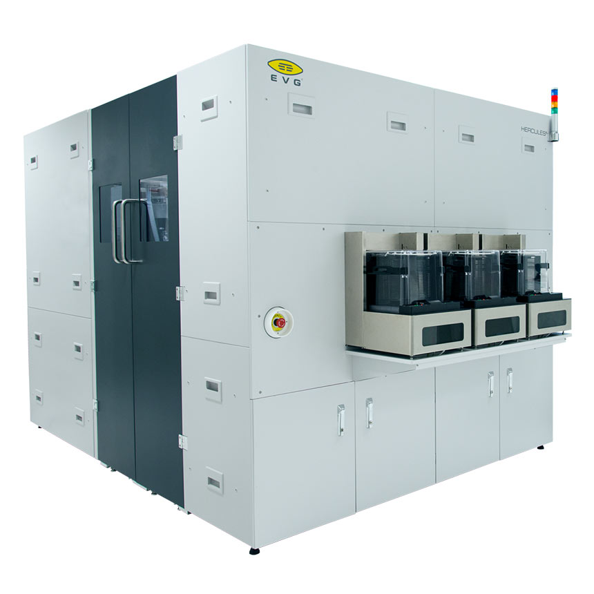
HERCULES® NIL fully integrated SmartNIL® UV-NIL system up to 200 mm
Integrated platform for pilot line and high-volume manufacturing with SmartNIL® up to 200 mm
The HERCULES NIL 200mm is the industry standard for nanoimprint lithography in high volume manufacturing. Based on a modular platform, the HERCULES NIL combines EVG’s proprietary SmartNIL imprinting technology with cleaning, resist coating and baking pre-processing steps. The configuration is tunable and adjusted to provide at low cost the best throughput with low footprint. The Hercules NIL is equipped with the state of the art handling systems for most efficient processing on a 200mm platform.
To optimize the process chain, the fabrication of multiple-use soft stamps – which are a cornerstone for high-volume production – is included in the HERCULES NIL without requiring additional imprint stamp manufacturing equipment. The system supports the production of a variety of devices and applications, including optical devices for augmented/virtual reality (AR/VR) headsets, 3D sensors, bio-medical devices, nanophotonics, plasmonics and metasurfaces. By providing a complete NIL solution for high-volume manufacturing, the HERCULES NIL strengthens EVG’s leadership position in full-area NIL equipment solutions.
Features
- Volume-proven imprinting technology with superior replication fidelity
- Combines pre-processing (clean / coat / bake / chill) and SmartNIL®
- Up to 4 pre-processing modules
- Wafer sizes up to 200mm
- Fully automated imprinting and controlled low-force detachment for maximum working stamp reusability
- Fully recipe-controlled processing
- Volume manufacturing of structures down to 40 nm* and smaller
- Optional chuck with heating function
- Optional mini-environment
- Includes working stamp manufacturing capability
- Fastest curing times due to high-power light source
- Optimized modular platform for high throughput
*resolution dependent on process and template
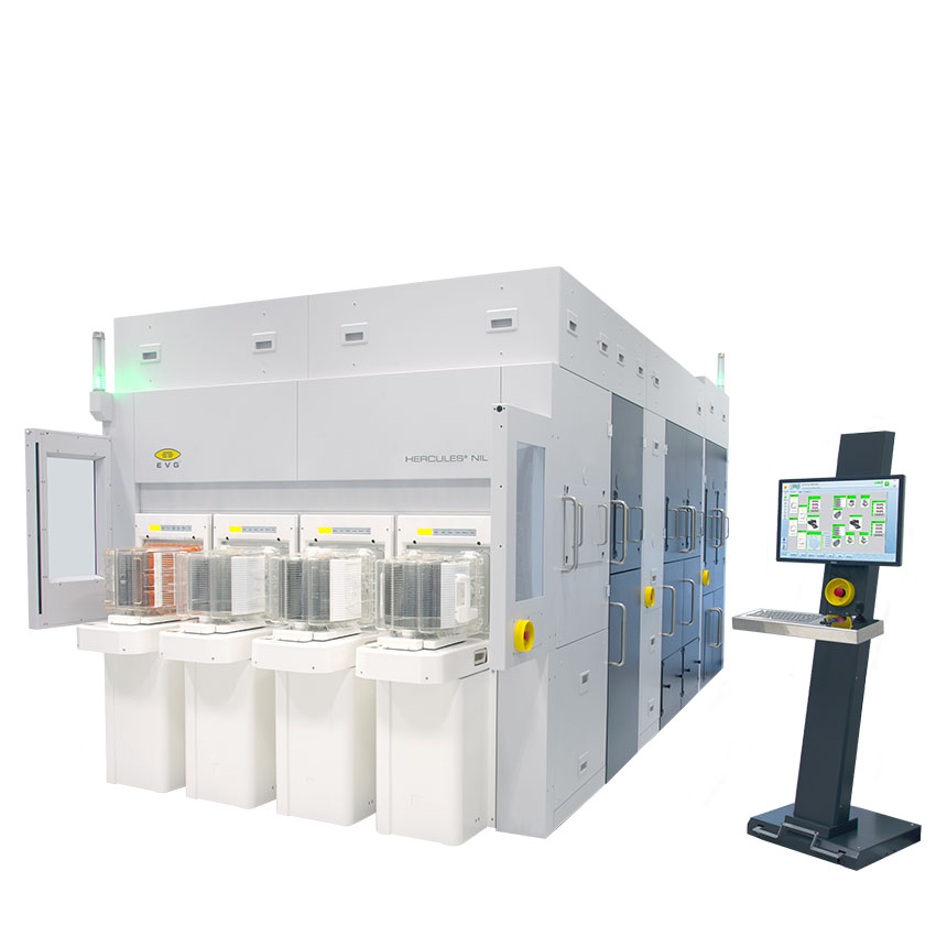
HERCULES® NIL fully modular and integrated SmartNIL® UV-NIL system up to 300 mm
Fully modular and integrated platform for pilot line and high-volume manufacturing with SmartNIL® up to 300 mm
The HERCULES NIL 300 mm is the first fully modular nanoimprint lithography system for high volume manufacturing. The system combines EVG’s proprietary SmartNIL imprinting technology with cleaning, resist coating and baking on a 300 mm platform. With the integration of the SmartNIL module and implementations of new hardware and software features, the HERCULES NIL 300 mm provides the most advanced nanoimprint capabilities on the market with low force and conformal imprinting, fast high-power exposure and smooth stamp detachment.
To optimize the process chain, the fabrication of multiple-use soft stamps – which are a cornerstone for high-volume production – is included in the HERCULES NIL without requiring additional imprint stamp manufacturing equipment. The system supports the production of a variety of devices and applications, including optical devices for augmented/virtual reality (AR/VR) headsets, 3D sensors, bio-medical devices, nanophotonics, plasmonics and metasurfaces. By providing a complete NIL solution for high-volume manufacturing, the HERCULES NIL strengthens EVG’s leadership position in full-area NIL equipment solutions.
Features
- Fully modular platform with up to eight swappable process modules (imprinting and pre-processing)
- Possibility to align several SmartNIL modules
- Up to 300 mm substrates
- 200 mm / 300 mm bridge-tool capability
- Fully automated UV-NIL imprinting and low-force detachment
- Temperature control unit with cooling system
- Full-area imprint coverage
- Volume manufacturing of structures down to 40 nm* and smaller
- Supports a wide range of structure sizes and shapes, including 3D
- Applicable on high-topography (rough) surfaces
*resolution dependent on process and template
Technical Data
| Wafer diameter (substrate size) |
|---|
| 100 up to 200 mm / 200 and 300 mm |
| Resolution |
|---|
| ≤ 40 nm (resolution dependent upon template and process) |
| Supported Process |
|---|
| SmartNIL® |
| Exposure source |
|---|
| High-power narrow-band |
| Alignment |
|---|
| ≤ ± 3 µm |
| Automated separation |
|---|
| Supported |
| Pre-processing |
|---|
| All pre-processing modules available |
| Mini environment and climate control |
|---|
| Optional |
| Working stamp fabrication |
|---|
| Supported |
Related downloads

Talk to our EVG product experts!
Questions?
Related technologies
Questions about our products and technologies?
Contact the EVG experts

