- Produkte
-
Technologien
- IR LayerRelease™ Technology
- MLE™ - Maskless Exposure Technologie
- Nanopräge-Lithographie (NIL) - SmartNIL®
- Wafer-Level Optics
- Optische Lithographie
- Fotolackverarbeitung
- Temporäres Bonden und De-Bonden
- Eutektisches Bonden
- Transient Liquid Phase (TLP) Bonden
- Anodisches Bonden
- Metall-Diffusionsbonden
- Hybrid- und Fusionsbonden
- Die-to-Wafer Fusion and Hybrid Bonding
- ComBond® Technologie
- Metrologie
- Unternehmen
- Karriere
Optical Lithography
EV Group offers a complete portfolio to support the wide range of possibilities inherent in lithography technology.
Introduction
Optical lithography, the structuring of photosensitive materials by mask-defined light for subsequent semiconductor processes, is a well-known and established technology. Today’s main requirements for optical lithography are defined by several key parameters. Sub-micron alignment accuracy, controlled uniform proximity gap between mask and wafer, as well as a clearly defined and precisely controlled exposure spectrum corresponding to the resist sensitivity, are among the most important criteria taken into account. Additionally, EVG´s customer-focused approach includes customized solutions for dedicated process needs. Understanding special requirements and having the flexibility to adapt our systems accordingly are among the unique core competences that EVG brings to the marketplace while constantly enhancing its lithography portfolio.
Related technologies
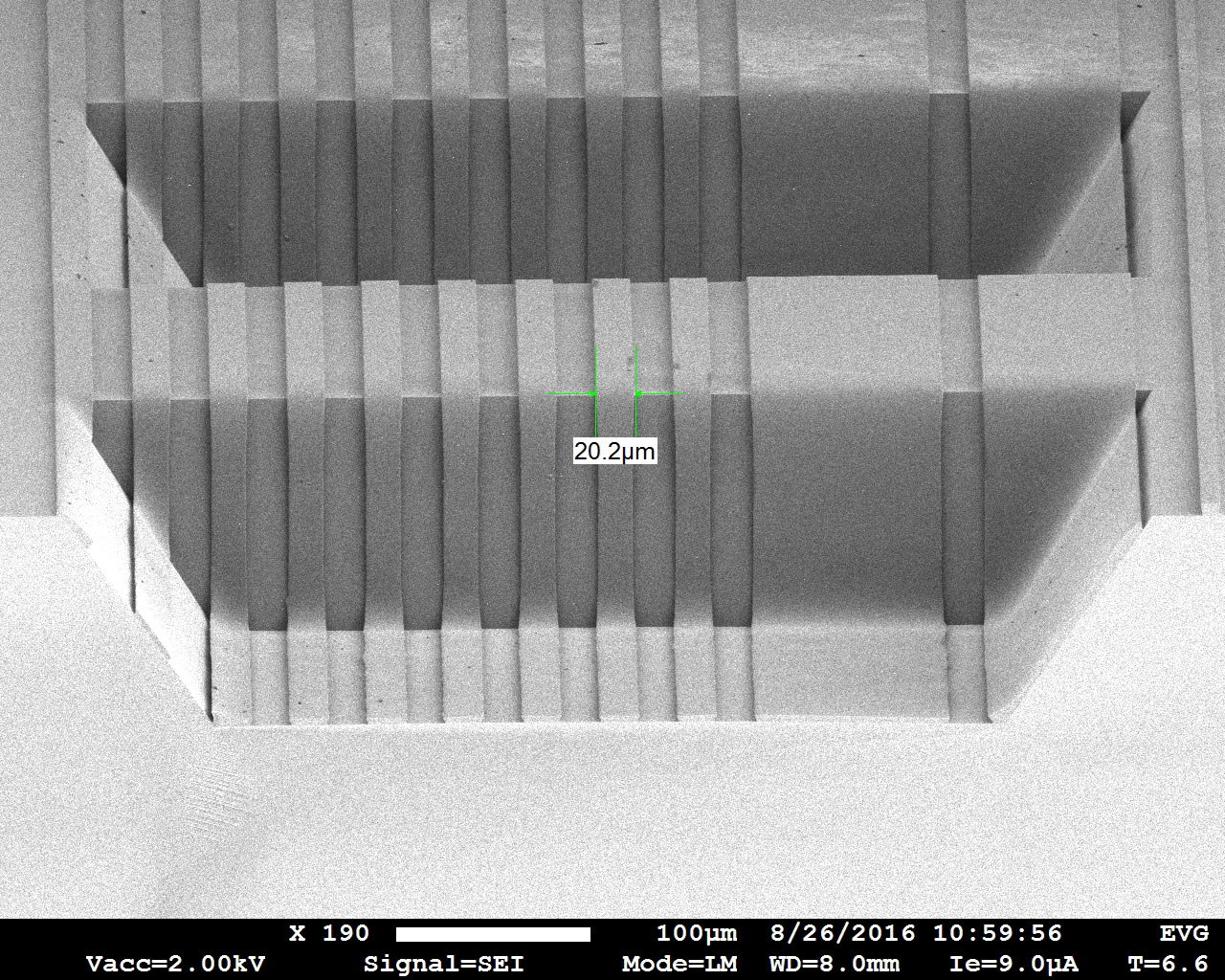
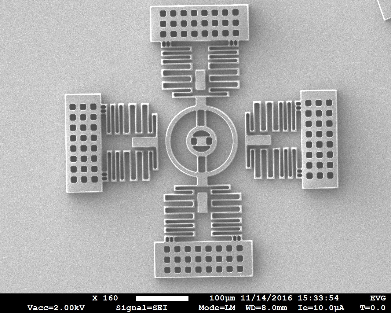
Over the years, optical lithography has continued to evolve to meet the scaling requirements for new semiconductor device designs. EVG has also continuously looked ahead at future market requirements and developed new innovations in the field of optical lithography technology – from the invention of the world’s first double-sided mask aligner in 1985 up to today, with the IQ Aligner NT achieving a top-side alignment down to 250 nm. Furthermore, EVG has implemented many advanced alignment features, such as runout control with temperature-controlled toolset, automatic cross correction, full clearfield mask movement, edge alignment and dynamic alignment. The latest implemented technology in EVG’s mask alignment product family is UV-LED technology, which gives users much more flexibility for their applications in terms of UV exposure spectrum setup, as spectral lines are individually tunable and special optical filters are no longer required. Maintenance of UV-LED lamp houses is also minimized. Further capabilities such as bond, transmissive or reflective IR alignment, as well as EVG’s proprietary SmartNIL technology, make EVG’s mask aligners very well equipped and advanced. This technology is well-established in the worldwide market today, covering all essential steps and able to serve various applications, such as wafer bumping, creation of redistribution layer (RDL) and via etching masks, via bottom opening processes, as well as lithography performed on thin or temporary bonded wafers. Such systems can be configured in semi-automated configurations for R&D as well as fully automated system configurations running cassette-to-cassette processes for high-volume production.
Features
- Alignment modes
- Top-side alignment
- Bottom-side alignment
- IR alignment: transmissive or reflective
- Bond alignment
- NIL alignment
- Exposure source
- Mercury light source
- UV LED light source
- Exposure setup
- Vacuum contact | Hard contact | Soft contact | Proximity mode
- Flex mode allowing stage/mask movement during exposure
- Wedge compensation assuring uniform exposure results
- Fully automatic – SW controlled with various control options
- Contactless with proximity spacers
- Recipe controlled contact force [5 N – 80 N]
- Various advanced alignment features using sophisticated algorithms for overall alignment improvement down to 250 nm, offset correction, runout control or edge alignment
- System control including file sharing and back-up solution, un-limited number of recipes, multi-language user GUI and support, real-time remote access, diagnostics and troubleshooting
- Industrial automation features
- Cassette, SMIF, FOUP, SECS/GEM, thin, bowed, warped, edge wafer handling
- Nanoimprint lithography technology capability
- Smart process control and data analysis features including integrated analysis features for processes and machine control, parallel task/queueing task processing feature, equipment and process performance tracking feature, smart handling, occurrences and alarm analysis together with smart maintenance management and tracking
Related downloads
Related products
Kontaktieren Sie unsere EVG-Technologieexperten!
Fragen?
Events
Semicon South East Asia 2026
Besuchen Sie unseren Stand #1126 und hören Sie sich unseren Vortrag “Advanced Lithography Technologies for Packaging: Enabling Next Gen Plasma Dicing Applications” auf der Techstage am 06. Mai gehalten von Deputy Process Technology Manager Europe Tobias Zenger an.

9th International Workshop on Low Temperature Bonding for 3D Integration LTB-3D 2026
Hören Sie sich unseren Vortrag über “Xenon vs Argon Ion Activation for Room‑Temperature Wafer Bonding of Si and SiC” an, gehalten von Senior Process Technology Engineer Peter Kerepesi.
Weitere Informationen finden Sie hier.

ITF World 2026
Besuchen Sie unseren Stand auf der IMEC ITF World 2026!
- IR LayerRelease™ Technology
- MLE™ - Maskless Exposure Technologie
- Nanopräge-Lithographie (NIL) - SmartNIL®
- Wafer-Level Optics
- Optische Lithographie
- Fotolackverarbeitung
- Temporäres Bonden und De-Bonden
- Eutektisches Bonden
- Transient Liquid Phase (TLP) Bonden
- Anodisches Bonden
- Metall-Diffusionsbonden
- Hybrid- und Fusionsbonden
- Die-to-Wafer Fusion and Hybrid Bonding
- ComBond® Technologie
- Metrologie
Fragen zu unseren Technologien?
Kontaktieren Sie die EVG-Experten
