- Produkte
-
Technologien
- IR LayerRelease™ Technology
- MLE™ - Maskless Exposure Technologie
- Nanopräge-Lithographie (NIL) - SmartNIL®
- Wafer-Level Optics
- Optische Lithographie
- Fotolackverarbeitung
- Temporäres Bonden und De-Bonden
- Eutektisches Bonden
- Transient Liquid Phase (TLP) Bonden
- Anodisches Bonden
- Metall-Diffusionsbonden
- Hybrid- und Fusionsbonden
- Die-to-Wafer Fusion and Hybrid Bonding
- ComBond® Technologie
- Metrologie
- Unternehmen
- Karriere
ComBond® High Vacuum Wafer Bonding Technology
A breakthrough technology driving the bonding of “anything on anything” enabling emerging and “beyond CMOS” device designs
Introduction
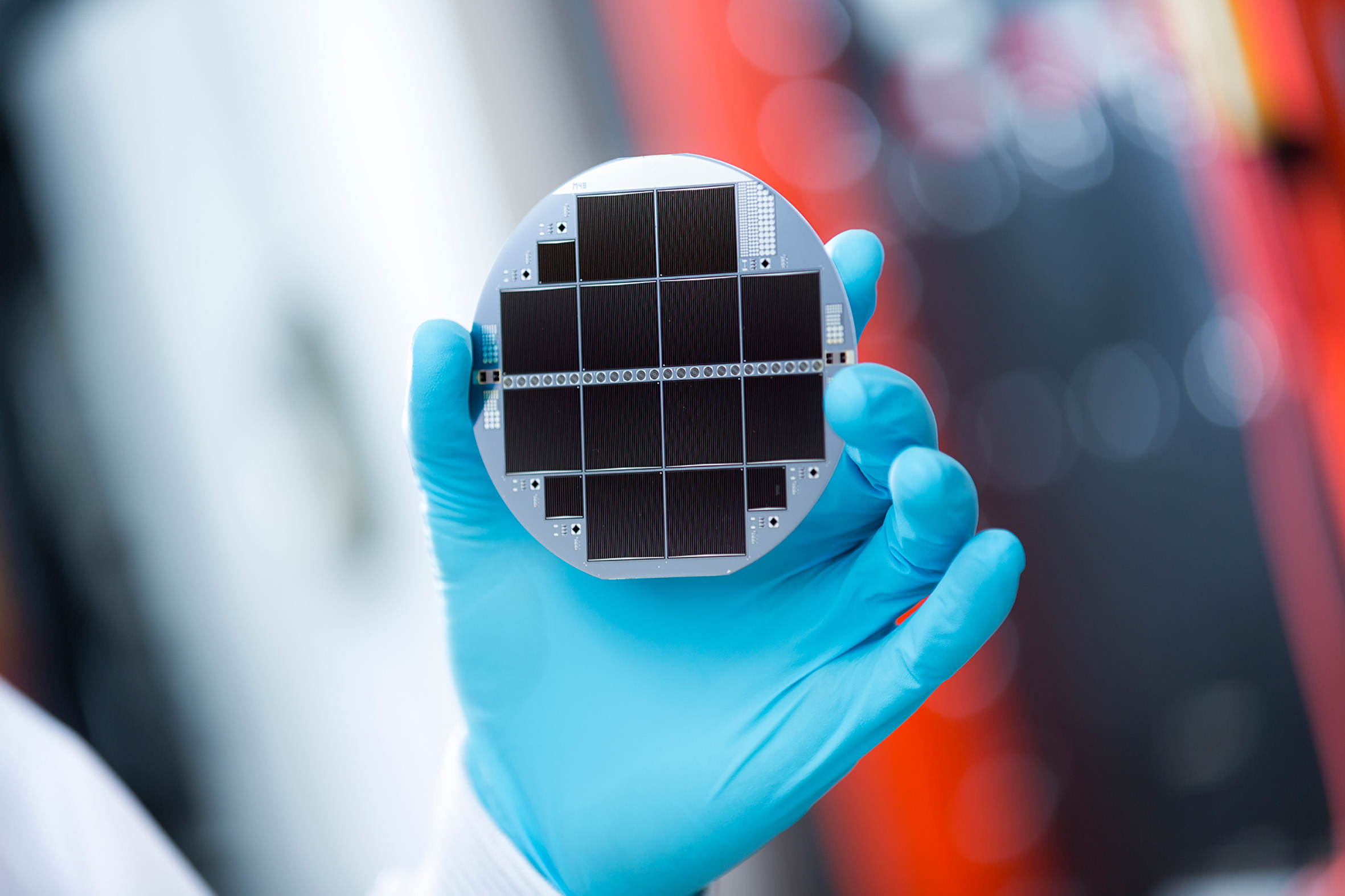
The ComBond technology adds a new milestone to EVG’s unique portfolio of wafer bonding equipment and technology in response to market needs for more sophisticated integration processes. The application areas range from advanced engineered substrates to high-end MEMS packaging, from “beyond CMOS” devices to stacked solar cells, and from high-performance logic to power devices.
The ComBond platform combines several technology breakthroughs to enable the formation of bond interfaces between heterogeneous materials at room temperature while achieving excellent bonding strength and electrical conductivity. Furthermore, ComBond enables the encapsulation of MEMS devices in high vacuum. Its capabilities include optical alignment with wafer clamping, programmable dehydration bake and getter activation, bonding in a bond chamber, and wafer handling done under high vacuum.
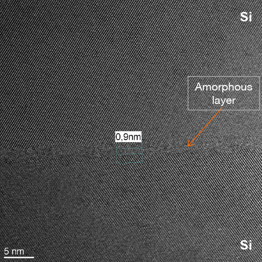
EVG’s breakthrough wafer activation technology and high-vacuum handling and processing allows the formation of covalent bonds at room or low temperature for the fabrication of engineered substrates and device structures. ComBond facilitates the bonding of heterogeneous materials with different lattice constant and coefficient of thermal expansion (CTE) as well as the formation of electrically conductive bond interfaces by its unique oxide-removal process. The ComBond high-vacuum technology also enables low-temperature bonding of metals, such as aluminum, that re-oxidize very fast in ambient environments. Void-free and particle-free bond interfaces and excellent bond strength can be achieved for all material combinations.
For vacuum encapsulation using aligned wafer bonding, the ComBond system advances its bonding capability through the addition of programmable dehydration bake and getter activation modules and the optical alignment module with wafer clamping. The high-vacuum handling and processing platform addresses rising demands for lower vacuum levels in leading-edge MEMS and other applications.
Market applications demanding room-temperature bonding of substrates with very different material properties include advanced engineered substrates, power devices, stacked solar cells and MEMS devices. The novel oxide-free bonding technique is particularly beneficial in silicon photonics, high-vacuum MEMS packaging, and compound semiconductor and other advanced engineered substrates for “beyond CMOS” applications such as high-mobility transistors, high-performance/low-power logic and radio frequency (RF) devices.
Features
- High-vacuum handling and processing (<7E-8 mbar) of wafers up to 200 mm
- Wafer surface activation
- Oxide-free direct bonding
- Room-temperature direct bonding
- Vacuum alignment capability
- Dehydration and bake-out of MEMS cavities
- High-vacuum encapsulation without getters
Related products

Kontaktieren Sie unsere EVG-Technologieexperten!
Fragen?
Events
Semicon South East Asia 2026
Besuchen Sie unseren Stand #1126 und hören Sie sich unseren Vortrag “Advanced Lithography Technologies for Packaging: Enabling Next Gen Plasma Dicing Applications” auf der Techstage am 06. Mai gehalten von Deputy Process Technology Manager Europe Tobias Zenger an.

9th International Workshop on Low Temperature Bonding for 3D Integration LTB-3D 2026
Hören Sie sich unseren Vortrag über “Xenon vs Argon Ion Activation for Room‑Temperature Wafer Bonding of Si and SiC” an, gehalten von Senior Process Technology Engineer Peter Kerepesi.
Weitere Informationen finden Sie hier.

ITF World 2026
Besuchen Sie unseren Stand auf der IMEC ITF World 2026!
- IR LayerRelease™ Technology
- MLE™ - Maskless Exposure Technologie
- Nanopräge-Lithographie (NIL) - SmartNIL®
- Wafer-Level Optics
- Optische Lithographie
- Fotolackverarbeitung
- Temporäres Bonden und De-Bonden
- Eutektisches Bonden
- Transient Liquid Phase (TLP) Bonden
- Anodisches Bonden
- Metall-Diffusionsbonden
- Hybrid- und Fusionsbonden
- Die-to-Wafer Fusion and Hybrid Bonding
- ComBond® Technologie
- Metrologie
Fragen zu unseren Technologien?
Kontaktieren Sie die EVG-Experten

