DE
Deutsch (DE)
Menü
- Produkte
-
Technologien
- IR LayerRelease™ Technology
- MLE™ - Maskless Exposure Technologie
- Nanopräge-Lithographie (NIL) - SmartNIL®
- Wafer-Level Optics
- Optische Lithographie
- Fotolackverarbeitung
- Temporäres Bonden und De-Bonden
- Eutektisches Bonden
- Transient Liquid Phase (TLP) Bonden
- Anodisches Bonden
- Metall-Diffusionsbonden
- Hybrid- und Fusionsbonden
- Die-to-Wafer Fusion and Hybrid Bonding
- ComBond® Technologie
- Metrologie
- Unternehmen
- Karriere
Suche
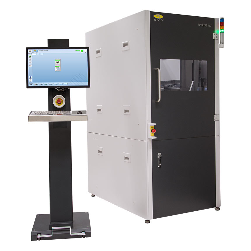
EVG®810 LT
LowTemp™ Plasma Activation System
Low-temperature plasma activation system for SOI, MEMS, compound semiconductors and advanced substrate bonding
The EVG810 LT LowTemp™ plasma activation system is a single-chamber, stand-alone unit with manual operation. The process chamber allows for ex-situ processes (wafers are activated one by one and bonded outside the plasma activation chamber). The EVG810 LT system can be combined with EVG's cleaning and bonding systems to enable a manual operation direct bonding process.
Features
- Surface plasma activation for low-temperature bonding (fusion/molecular and intermediate layer bonding)
- Fastest kinetics of any wafer bonding mechanism
- No wet processes required
- Highest bond strength at low temperature annealing (up to 400 °C)
- Applicable for SOI, MEMS, compound semiconductors, and advanced substrates bonding
- High degree of materials compatibility (including CMOS)
Technical Data
| Wafer diameter (substrate size) |
|---|
| 50 - 200, 100 - 300 mm |
| LowTemp™ plasma activation chamber |
|---|
| Process gases: 2 standard process gases (N2 and O2) |
| Universal mass flow controller: self-calibrating (up to 20.000 sccm) |
| Vacuum system: 9x10⁻² mbar |
| Opening / closing of chamber: automated |
| Loading / unloading of chamber: manual (wafer / substrate placed on loading pins) |
| Optional features |
|---|
| Chuck for different wafer sizes |
| Metal ion-free activation |
| Additional process gases with gas mixing |
| High vacuum system with turbo pump: 9x10⁻³ mbar base pressure |
| Material systems that are qualified with LowTemp™ plasma activated bonding |
|---|
| Si: Si/Si, Si/Si (thermally oxidized, Si (thermally oxidized)/Si (thermally oxidized) |
| TEOS/TEOS (thermally oxidized) |
| Si/Ge for Germanium-on-Insulator (GeOI) |
| Si/Si3N4 |
| Glass (borofloat, non-alkali): Si/Glas, Glass/Glass |
| Compound semiconductors: GaAs, GaP, InP |
| Polymers: PMMA, Cyclo Olefin Polymers |
| Best Known Method recipes available for users for the above and for other materials (full list available on request) |

Talk to our EVG product experts!
Questions?
Related technologies
Questions about our products and technologies?
Contact the EVG experts
Themenbezogene News
EV Group erreicht Spitzenposition bei der TechInsights Kundenzufriedenheitsumfrage 2025 für die weltweite Halbleiterindustrie
Jun, 2025
EV Group bringt mit dem LITHOSCALE® XT die digitale Lithographie in die Hochvolumenproduktion von heterogenen Integrationsanwendungen
May, 2025
EV Group gründet Niederlassung in Singapur zur Stärkung des lokalen Customer Supports
May, 2025
