临时键合和解键合
Temporary bonding and debonding enabling backside processing for 3D integration
Introduction
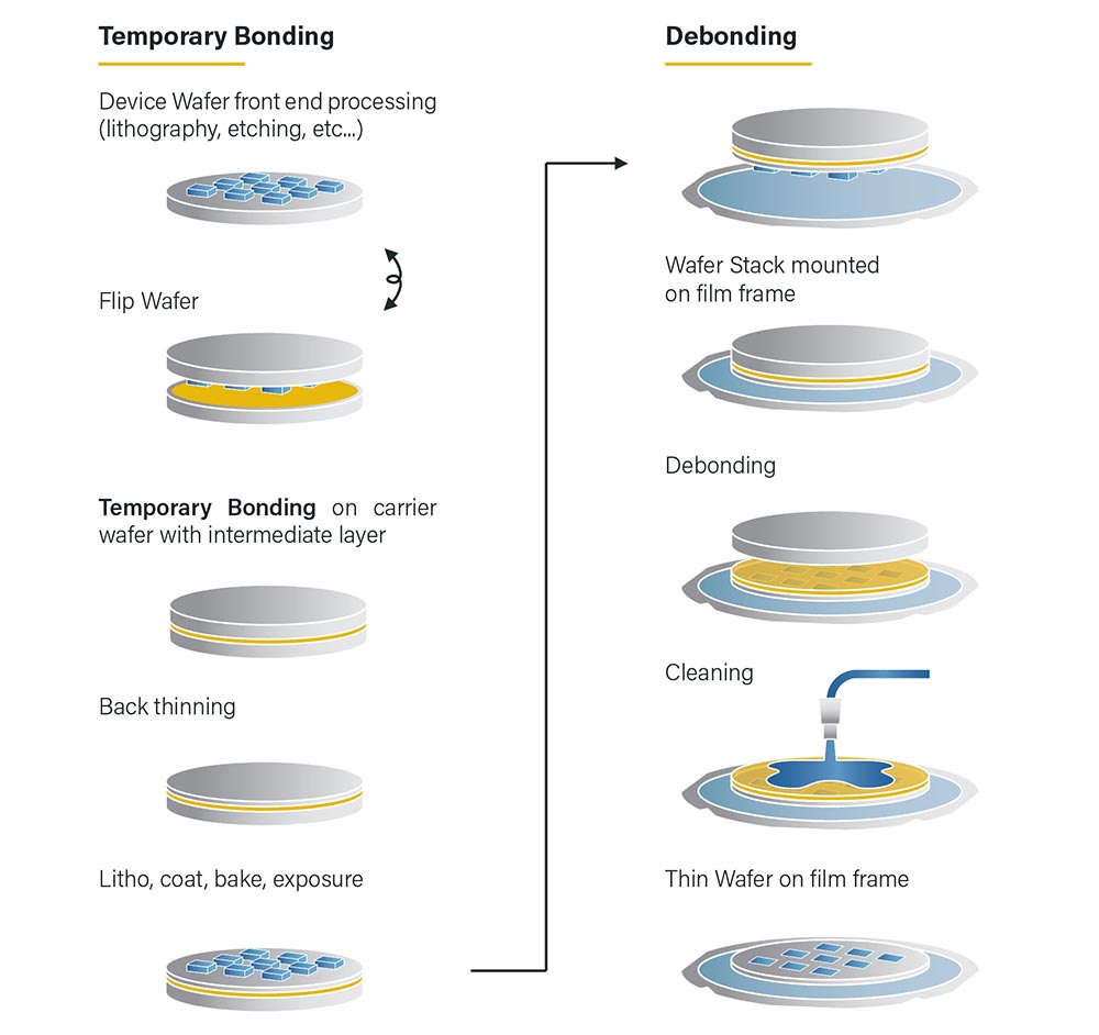
Temporary bonding is an essential process for enabling wafer thinning and for supporting thin-wafer transfer. This is key for advanced packaging, including 2.5D, 3D IC and Fan-out Wafer-level Packaging (FoWLP) wafers, for power devices, as well as for handling fragile substrates like compound semiconductors and MEMS wafers. EVG’s outstanding wafer bonding know-how includes temporary bonding and debonding equipment, which EVG has been providing to leading fabs, foundries and packaging companies since 2001.
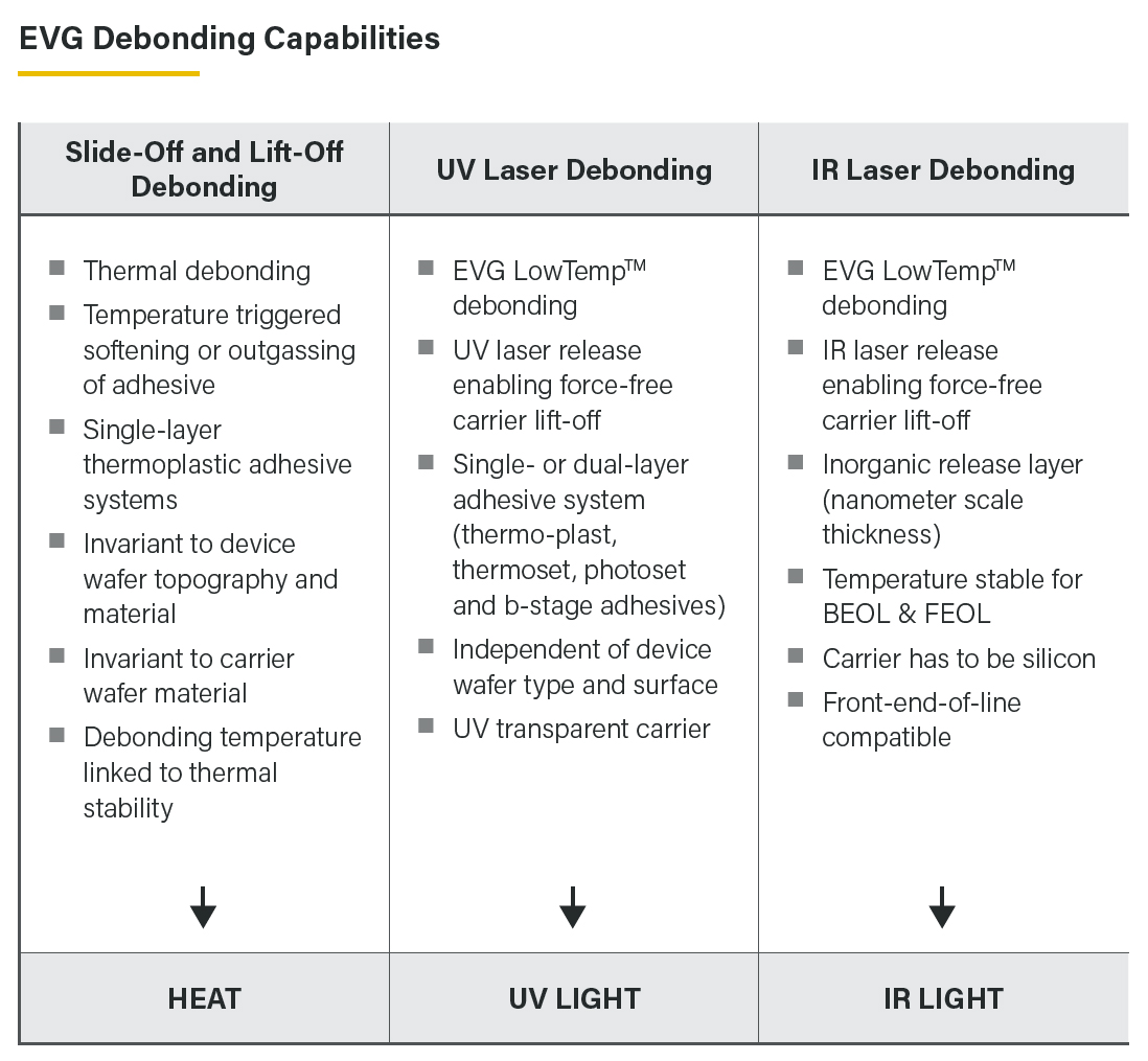
EVG’s most recent innovations in debonding technologies are UV and IR laser debonding, with a wide process window and LowTemp debonding for smooth process integration, enabling the production of ultra-thin chips and packages for next-generation devices. These debonding technologies complement EVG’s thermal slide-off debonding, which was the first debonding technology implemented in HVM production for advanced packaging.
EVG’s open adhesive platform, that supports all commercially available adhesive materials in combination with the different debonding technologies, enables tailored solutions for a wide range of applications with special requirements.
- Thermal slide-off debonding utilizes the softening of thermoplastic adhesives at elevated temperatures to separate the device wafer from the carrier.
- UV laser debonding separates the device wafer and the UV transparent carrier wafer by decomposing the UV laser release layer without risking the device wafers’ integrity.
- IR laser debonding (LayerRelease) is compatible with silicon carrier wafers with an inorganic IR laser release layer, which is cleanable with inorganic solvents.
Features
- Open adhesive platform
- Thermal Slide-Off, UV Laser or IR Layer Release Debonding
- Modular tool layout for throughput optimization
- Bridge capability for different substrate sizes
- Available with multiple load port options and combinations
- Film Frame, stand-alone wafer, or thin-wafer carrier as output options
- Integrated metrology enables feedback loop for high-yield processes in automated tools
- Software monitoring of the whole process for equipment performance tracking
- Fully integrated SECS/GEM interface in automated tool
Related products
Talk to our EVG technology experts!
Questions?
Events
250th ECS Meeting
Listen to our talks: "Simulation-Informed Real-Time Wafer-to-Wafer Bonding Process Control under Varying Surface Conditions" held by Dr. Lukas Koller from our Process Modelling & Simulation Team and “Low Temperature Plasma Treated Silicon Nitride Based Dielectrics for Direct Wafer Bonding Processes” held by Deputy Team Leader Process Technology - Fusion Bonding David Doppelbauer.
Here you'll find the program.
SEMICON Europa 2026
Visit our booth #B1241 at SEMICON EUROPA 2026 & our poster presentations at the APC:
“Software-Driven Strategies for Advanced Multi-Die Patterning in Digital Lithography “ presented by Business Development Manager Dr. Ksenija Varga and ”Leveraging Advanced Bonding Technologies to Enable Scalable Co-Packaged Optics Architectures” introduced by Business Development Manager Elisabeth Brandl.
Here you'll find more Information on the program.
Industrial Print Integration Conference (IPI) 2026
Listen to our Keynote “Advancing AR/VR and CPO: EV Group’s Inkjet Solutions for Next-Generation Optics” held byJohanna Rimböck (Technology Development).
For more information about the program click here.
Questions about our technologies?
Contact the EVG experts