涂胶工艺技术
Resist processing technology together with patterning are the most repeated steps in semiconductor manufacturing.
Introduction
Resist processing technology is widely used for numerous micro- and nanotechnology applications and products addressing different markets, such as advanced packaging, MEMS, MOEMS and sensors, microfluidics, RF devices, photonics and many more. All these application fields bring new challenges for semiconductor device design and manufacturing. Understanding these special requirements and having the flexibility to adapt our systems accordingly are among the unique core competences that EVG brings to the marketplace.
Related technologies
Important advancements by EV Group in lithography technology include proprietary resist coating technologies, such as OmniSpray, revolutionary NanoSpray and NanoFill. These unique technologies are implemented in the EVG100 series of resist processing systems and establish new standards in quality and flexibility for photoresist coating and developing. Designed to support a wide range of process parameters and customer requirements, an extensive range of materials – such as positive and negative resists, polyimides, double-sided coating of thin-resist layers, high-viscosity resists, and edge-protection coatings – can be processed on the EVG100 series. While the importance of resist processing to enable certain process flows is often underestimated and just considered a commodity for standard lithography processes, in many cases it is the key enabling process. For example, patterning on high-topography wafers, LIGA (lithography, electroforming, and molding), temporary bonding, nanoimprint lithography (NIL) and adhesive bonding all rely on advanced coating capabilities and process excellence. EVG has built up many years of spin and spray coating experience for demanding applications and incorporates these learnings into the EVG100 series, where our process know-how can be leveraged to support our customers. As with all EVG processing systems, the equipment can be configured for R&D environments or for high-volume production.
Features
- Wafer sizes supported up to 300 mm
- Coating of up to 52,000 cP enables manufacturing of ultra-thick resist features of up to 300 µm with an extensive range of supported materials
- Available modules
- Spin coat module with a simulation-based low-turbulence design
- OmniSpray® coating for optimized coating of high-topography surfaces
- NanoSpray™/NanoFill™ for coating/filling and protection of via structures
- Develop
- Bake
- Chill
- Vapor
- CoverSpin™ rotating cover for low resist consumption and optimized resist coating uniformity
- EV Group's proprietary OmniSpray® ultrasonic atomization technology provides unmatched conformal coating process results on extreme topographies
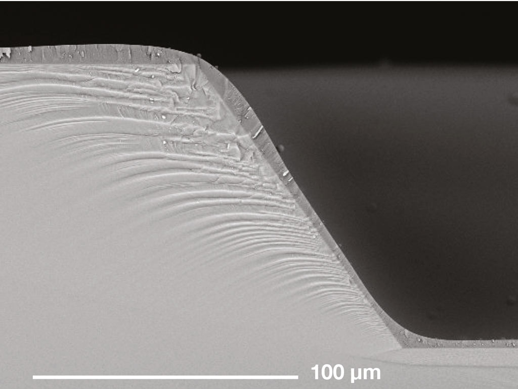
- Optional NanoSpray™ module achieves conformal coating of 300 µm deep patterns with aspect ratios up to 1:10 and vertical sidewalls
- Easy process transfer from research to production utilizing proven modular design
- Fragile, thin or warped wafer handling of multiple wafer sizes
- Smart process control and data analysis software features
- Integrated analysis features for process and machine control
- Parallel task/queueing task processing feature
- Equipment and process performance tracking feature
- Smart handling features
- Occurrences and alarms analysis
- Smart maintenance management and tracking
- Multi-user concept (unlimited number of user accounts and recipes, assignable access rights, different user interface languages)

Talk to our EVG technology experts!
Questions?
Events
Semicon South East Asia 2026
Visit our booth #1126 and listen to our talk “Advanced Lithography Technologies for Packaging: Enabling Next Gen Plasma Dicing Applications” at the Techstage on 06th of May held by Deputy Process Technology Manager Europe Tobias Zenger.

9th International Workshop on Low Temperature Bonding for 3D Integration LTB-3D 2026
Listen to our talk “Xenon vs Argon Ion Activation for Room‑Temperature Wafer Bonding of Si and SiC” held by Senior Process Technology Engineer Peter Kerepesi.
More information here.

ITF World 2026
Visit our booth at ITF World 2026!
Questions about our technologies?
Contact the EVG experts
