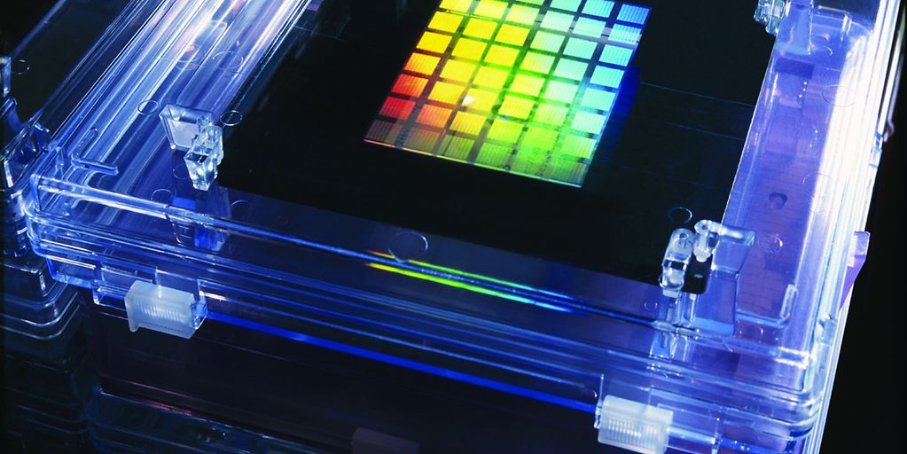
Spray Coating Technology
Spray coating technology is a valuable alternative resist deposition technique, which overcomes limitations of conventional spin coating technology.
Introduction
Spray coating technology provides several benefits and allows the ability to overcome remaining drawbacks of spin coating such as low material consumption, but more importantly can provide uniform coatings on non-planar surfaces or even inside the cavities, vias or trenches.
Related technologies
Although spin coating is still a preferred method of resist processing and a well-understood technology, this process has fundamental limitations with respect to device topography, material consumption, and oversized and fragile substrates. However, many applications often exhibit high topography variations. The surface planarity of the coated material significantly impacts further processes. For example, patterning on high-topography wafers, LIGA (lithography, electroforming, and molding), temporary bonding, nanoimprint lithography (NIL) and adhesive bonding rely on advanced coating capabilities and process excellence. Combining numerous requirements such as ultra-thin film thickness or flat surface – especially inside the cavities or vias – upsurges the process control complexity. Proprietary OmniSpray technology can fulfill such challenging requirements by providing excellent uniformity results. Its pressure-less ultrasonic atomization of the resist material guarantees precisely controlled droplet size and its narrow spectral distribution independent from N2 flow. Fully recipe-controlled spray nozzle parameters and x/y meander movement provide high flexibility and repeatability of the spray coating process. The optionally available heated chuck system can further extend the application range. Furthermore, NanoSpray/NanoFill technologies belong to other important advancements by EV Group. The patented multi-step NanoSpray process is a unique coating technique under vacuum conditions, enabling uniform resist coverage of a variety of via geometries and sidewalls for high aspect TSVs with ratio of up to 1:20. NanoFill technology allows complete, void-free filling of vias with flat surfaces. These novel coating processes enable applications like in-via lithography, fast and cost-efficient deposition of organic low-k dielectrics, and easy-to-remove in-via protective coatings. Moreover, EVG’s process technology excellence includes an extensive range of materials such as positive and negative resists, polyimides, double-sided coating of thin-resist layers, high-viscosity resists or resins containing nanoparticles, and is thus able to fulfill advanced process parameters challenged by current market demands.
Features
- Precise recipe-controlled resist dispensing process
- Pressure-less ultrasonic atomization of the resist material guarantees precisely controlled droplet size independent to N2 flow
- Narrow spectral droplet distribution
- Extensive range of photoresists with viscosities up to 52000 cP
- OmniSpray® advanced process control guaranteeing conformal resist coverage of a variety of via geometries, edge coverage and sidewalls for high aspect TSVs
- Optional NanoSpray™ module achieves conformal coating of 300µm deep patterns with aspect ratios up to 1:10 and vertical sidewalls
- Fragile, thin or warped wafer handling of multiple wafer sizes
- Process technology excellence and development service
- Smart process control and data analysis software features
- Integrated analysis features for process and machine control
- Parallel task/queueing task processing feature
- Equipment and process performance tracking feature
- Smart handling features
- Occurrences and alarms analysis
- Smart maintenance management and tracking


Talk to our EVG technology experts!
Questions?
Events
EMLC 2026
Listen to our talks on Wednesday June 22th in Session 4:
"Enhancing SWIR Device Fabrication Through Digital Lithography with Novel IR-Pass Resists" held by Business Development Manager Dr. Ksenija Varga and
"Challenges and Solutions for Flexible, Scalable, High-Throughput Digital" held by Senior Optical Systems Expert Dr. Boris Považay.
Leti Innovation Days 2026
Visit us at our booth at the Leti Innovation Days 2026!

ICEPT 2026
Listen to our presentation "Fusion & Hybrid Bonding: Driving Application Performance, Power and Cost by Mixing and Matching Semiconductor Technologies" held by Business Development Manager Dr. Thomas Pleschke.
Questions about our technologies?
Contact the EVG experts