EN
English (EN)
Menu
- Products
-
Technologies
- IR LayerRelease™ Technology
- MLE™ - Maskless Exposure Technology
- Nanoimprint Lithography (NIL) - SmartNIL®
- Wafer Level Optics
- Optical Lithography
- Resist Processing Technology
- Temporary Bonding and Debonding
- Eutectic Bonding
- Transient Liquid Phase (TLP) Bonding
- Anodic Bonding
- Metal Diffusion Bonding
- Hybrid and Fusion Bonding
- Die-to-Wafer Fusion and Hybrid Bonding
- ComBond® Technology
- Metrology
- Company
- Careers
Search
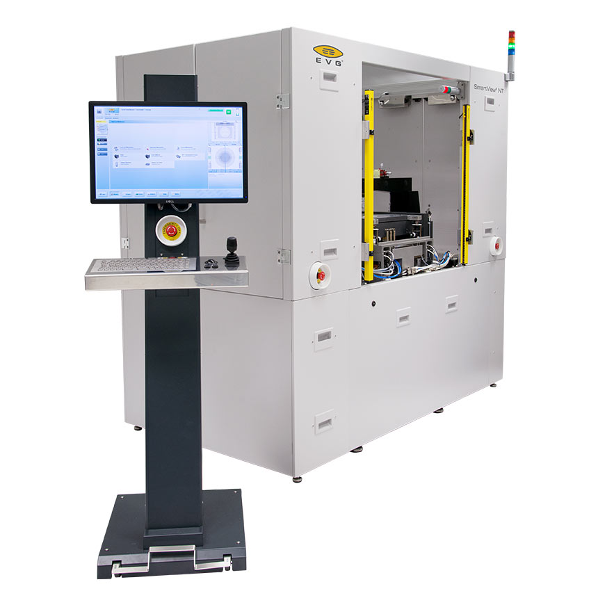
SmartView® NT
Automated Bond Alignment System for Universal Alignment
Fully automated bond alignment system for universal alignment with proprietary method for micron-level face-to-face wafer alignment
The SmartView NT automated bond alignment system for universal alignment offers a proprietary method for micron-level face-to-face wafer-level alignment. This alignment technique is key to achieving the required accuracy in multiple wafer stacks for leading-edge technologies. The tool is well suited for applications such as wafer stacking for 3D interconnects, wafer-level-packaging and high-volume MEMS devices.
Features
- Suitable for automated and integrated EVG bonding systems (EVG®560, GEMINI®) in 200 mm and 300 mm configurations
- Universal bond aligner (face-to-face-, backside-, infrared- and transparent alignment)
- No Z-axis motion and no refocusing required
- Windows® based user interface
- Bond pairs are aligned and clamped prior to loading into the bond chamber
- Manual or fully automated configurations (e.g. integration with GEMINI®)
- Options
- Can be combined with the EVG®500 series wafer bonding systems, EVG®300 series cleaning systems and EVG®810 LT plasma systems for a fully automated wafer-to-wafer alignment operation with cassette-to-cassette operation
Technical Data
| Substrate / Wafer parameters |
|---|
| Size: 150 - 200, 200 - 300 mm |
| Thickness: 0,1 - 5 mm |
| Max. stack height: 10 mm |
| Automatic alignment |
|---|
| Standard |
| Handling system |
|---|
| 3 cassette stations (up to 200 mm) or 2 FOUP load ports (300 mm) |

Talk to our EVG product experts!
Questions?
Questions about our products and technologies?
Contact the EVG experts
Related News
