EN
English (EN)
Menu
- Products
-
Technologies
- IR LayerRelease™ Technology
- MLE™ - Maskless Exposure Technology
- Nanoimprint Lithography (NIL) - SmartNIL®
- Wafer Level Optics
- Optical Lithography
- Resist Processing Technology
- Temporary Bonding and Debonding
- Eutectic Bonding
- Transient Liquid Phase (TLP) Bonding
- Anodic Bonding
- Metal Diffusion Bonding
- Hybrid and Fusion Bonding
- Die-to-Wafer Fusion and Hybrid Bonding
- ComBond® Technology
- Metrology
- Company
- Careers
Search
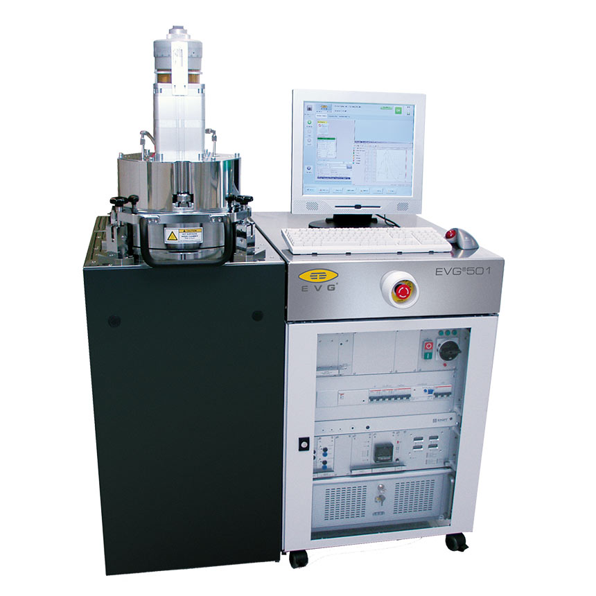
EVG®501
Wafer Bonding System
Versatile manual wafer bonding system for academia and industrial research
The EVG501 is a highly flexible wafer bonding system and supports all common wafer bonding processes such as anodic, glass frit, solder, eutectic, transient liquid phase, and direct. The easy access bond chamber and tooling design allows for quick and easy retooling for different wafer sizes and processes. This versatility is ideal for universities, R&D facilities, or low-volume production. The design of the bond chambers is similar to the EVG high-volume-manufacturing tools, such as the EVG GEMINI, and the bonding recipes are easily transferable, allowing for easy scale up of production volumes.
Features
- Unique pressure and temperature uniformity
- Compatible with EVG mechanical and optical aligners
- Flexible design and configurations for research
- From single chips to wafers
- Various processes (eutectic, solder, TLP, direct bonding)
- Optional turbopump (<1E-5mbar)
- Upgradeable for anodic bonding
- Open chamber design for easy conversion and maintenance
- Pilot production compatible
- Open chamber design for easy conversion and maintenance
- Smallest footprint for a 200 mm bonding system: 0.8 m2
- Recipes are fully compatible with EVG’s high-volume-manufacturing bonding systems
Technical Data
| Max contact force |
|---|
| 20 kN |
| Heater size | 150 mm | 200 mm |
|---|---|---|
| Minimum substrate dimension | single chips | 100 mm |
| Vacuum |
|---|
| Standard: 0.1 mbar |
| Optional: 1E-5 mbar |
| Max. temperature |
|---|
| 450 °C |
| Single chips processing |
|---|
| Yes |
| Bond chuck system / Alignment system |
|---|
| 150 mm heater: EVG®610, EVG®620, EVG®6200 |
| 200 mm heater: EVG®6200, SmartView® NT |
| Active water cooling |
|---|
| For bottom side |
| Power supply for anodic bonding |
|---|
| Max. voltage: 2 kV |
| Max. current: 50 mA |
| Loading chamber |
|---|
| Manual |

Talk to our EVG product experts!
Questions?
Questions about our products and technologies?
Contact the EVG experts
Related News
