金属扩散键合
Metal diffusion bonding for precise interfaces and alignment
Introduction
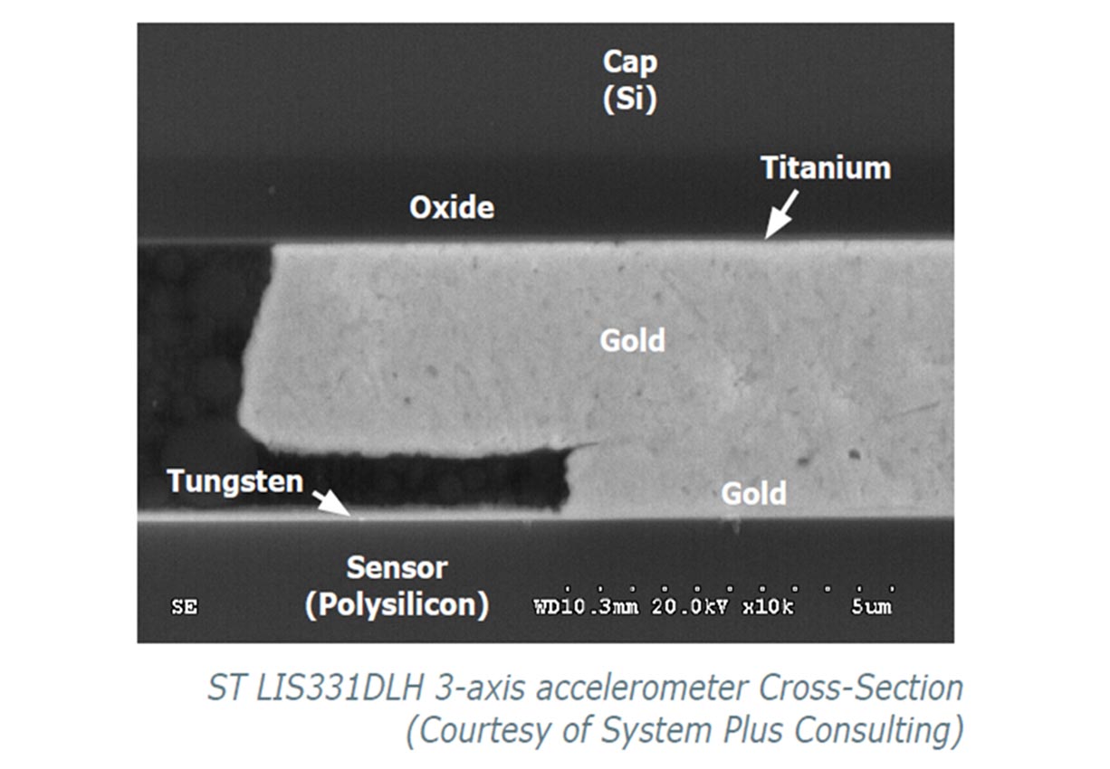
Metal diffusion bonding, also known as Thermo compression bonding (TCB), is a direct solid-state diffusion bonding process and is based on atomic contact. In this bonding technique, two metals are brought into contact by applying heat and force simultaneously after which the atoms diffuse to form the bond interface. TCB is widely used in the production of RF MEMS, light emitting diodes (LEDs), laser diodes as well as power devices.
TCB provides hermetic sealing of packaged internal structures and electrical interconnects in a single process step. Because of their high diffusion rates, Au, Al and Cu are the most established materials that are used in TCB. Compared to Al and Cu, Au requires less temperature for diffusion and has an added advantage of not becoming oxidized. The diffusion rate depends on the chosen temperature and applied pressure where the atoms diffuse between crystal lattices. Here, grain boundary and bulk diffusion takes place in addition to standard surface diffusion.
In this technology, wafer-level bonding is achieved at low temperatures without the application of an electric field. Nevertheless, good control of CTE (coefficient of thermal expansion) and synchronized wafer expansion is important to prevent any resulting stress and alignment shift during bonding. Furthermore, the applied force and its uniformity are important, which also depend on the metal density (features) and size of the wafers. In TCB, the bonding temperature and the applied pressure are inversely proportional, which gives a feasibility to tailor the bonding parameters.
Features
- Electrically conductive
- High fracture toughness
- Small bonding frames
- Hermetic sealing
- Very good post-bond alignment
- No contamination
- No or very little deformation

Talk to our EVG technology experts!
Questions?
Events

ICEP-HBS 2026
Listen to our talks:
“Hybrid Bonding and Interconnect Scaling: Driving Application Performance, Power and Cost by Mixing and Matching Semiconductor Technologies” by Representative Director Hiroshi Yamamoto.
“A predictive model for bond strengthening based on ion characteristics and the interface evolution in plasma activated fusion and hybrid bonding” by Deputy Team Leader Process Technology David Doppelbauer.
“From Scaling to Stacking: How Fusion and Hybrid Bonding enable Next-Generation High Performance Chip Architectures” by Business Development Manager Thomas Pleschke.
For more information click here.

Merck "The Future of Photonics — Materials Matter"
Listen to our talk “Enabling Scalable Photonic Packaging using Nanoimprint Lithography” held by Business Development Manager Andrea Kronawitter.
More information here.

CS / PIC / PE International Conference 2026
Visit us at our booth at the CS / PIC and PE International Conference and listen to our talks:
"High performance GaN power devices enabled by wafer bonding" held by Business Development Manager Elisabeth Brandl at the CS Conference.
"Advancing Photonic Packaging and Integration Through UV Nanoimprint Lithography" held by Senior Process Technology Engineer Patrick Schuster at the PIC Conference.
Questions about our technologies?
Contact the EVG experts

