- Products
-
Technologies
- IR LayerRelease™ Technology
- MLE™ - Maskless Exposure Technology
- Nanoimprint Lithography (NIL) - SmartNIL®
- Wafer Level Optics
- Optical Lithography
- Resist Processing Technology
- Temporary Bonding and Debonding
- Eutectic Bonding
- Transient Liquid Phase (TLP) Bonding
- Anodic Bonding
- Metal Diffusion Bonding
- Hybrid and Fusion Bonding
- Die-to-Wafer Fusion and Hybrid Bonding
- ComBond® Technology
- Metrology
- Company
- Careers
Mask Alignment Systems
EVG’s inventions, such as the world’s first bottom-side alignment system in 1985, have pioneered and set the industry standards in both top and double-sided lithography, aligned wafer bonding and nanoimprint lithography. EVG contributes in these areas through continuous development of mask aligner product generations to augment this core lithography technology.
Accommodating wafers and substrates up to 300 mm, varying in size, shape and thickness, EVG’s mask alignment systems aim to provide sophisticated solutions with a high grade of automation for advanced applications and full flexibility for research and development. EVG’s mask aligners as well as process competencies are field proven and installed in production facilities around the globe to support numerous applications, including advanced packaging, compound semiconductor, power device, LED, sensor and MEMS manufacturing.
Choose your Mask Alignment System
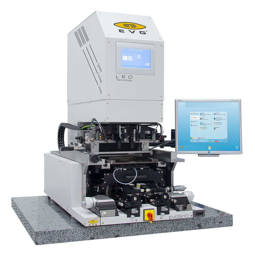
EVG®610
Mask Alignment System
Mask aligner designed for optical double-side lithography.
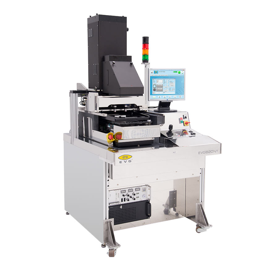
EVG®620 NT
Semi-automated / Automated Mask Alignment System
Mask aligner designed for optical double-side lithography.
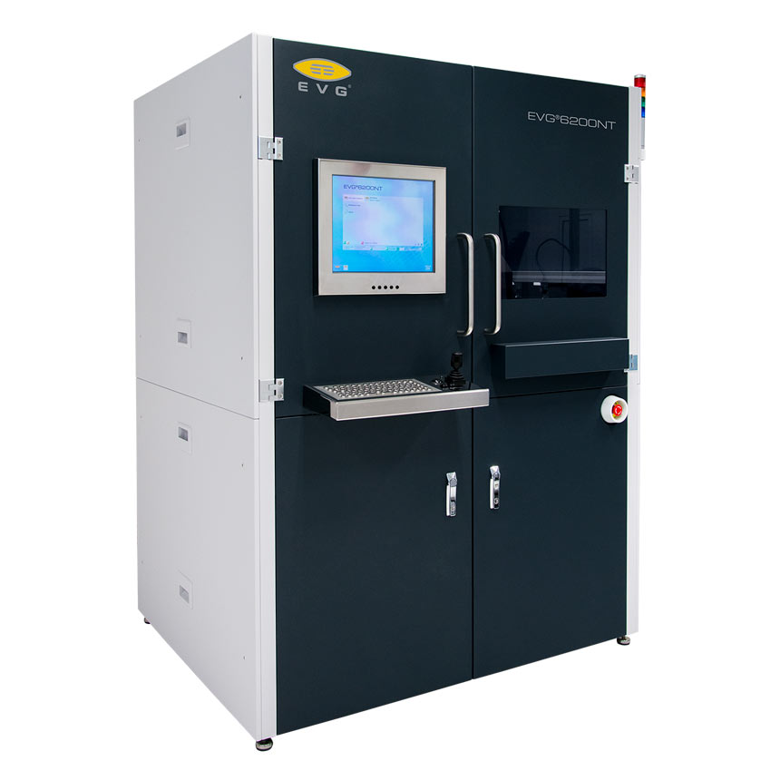
EVG®6200 NT
Semi-automated / Automated Mask Alignment System
Mask aligner designed for optical double-side lithography.

Talk to our EVG product experts!
Questions?
Questions about our products and technologies?
Contact the EVG experts
