DI Erich Thallner Strasse 1
4782 St. Florian am Inn
Austria
- Products
-
Technologies
- IR LayerRelease™ Technology
- MLE™ - Maskless Exposure Technology
- Nanoimprint Lithography (NIL) - SmartNIL®
- Wafer Level Optics
- Optical Lithography
- Resist Processing Technology
- Temporary Bonding and Debonding
- Eutectic Bonding
- Transient Liquid Phase (TLP) Bonding
- Anodic Bonding
- Metal Diffusion Bonding
- Hybrid and Fusion Bonding
- Die-to-Wafer Fusion and Hybrid Bonding
- ComBond® Technology
- Metrology
- Company
- Careers
Silicon Austria Labs and EV Group strengthen Collaboration in Optical Technology Research
Expanded collaboration includes installation of EVG’s LITHOSCALE® maskless exposure system, EVG®7300 UV-NIL system and complementary resist processing systems

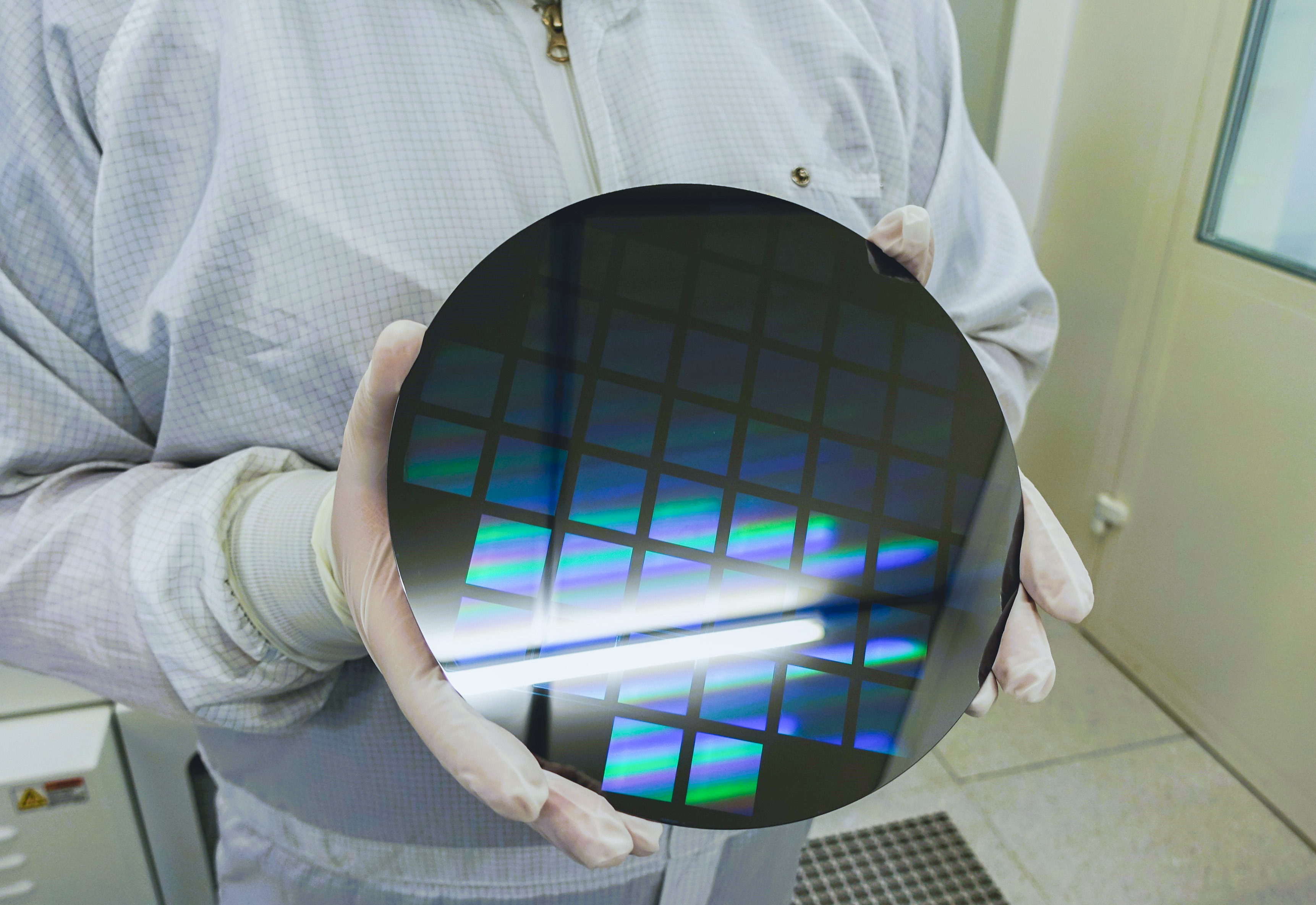
Exquisite nanoimprint master: pioneering precision for mass-production of meta-optics devices, showcasing intricate design and unprecedented fabrication prowess

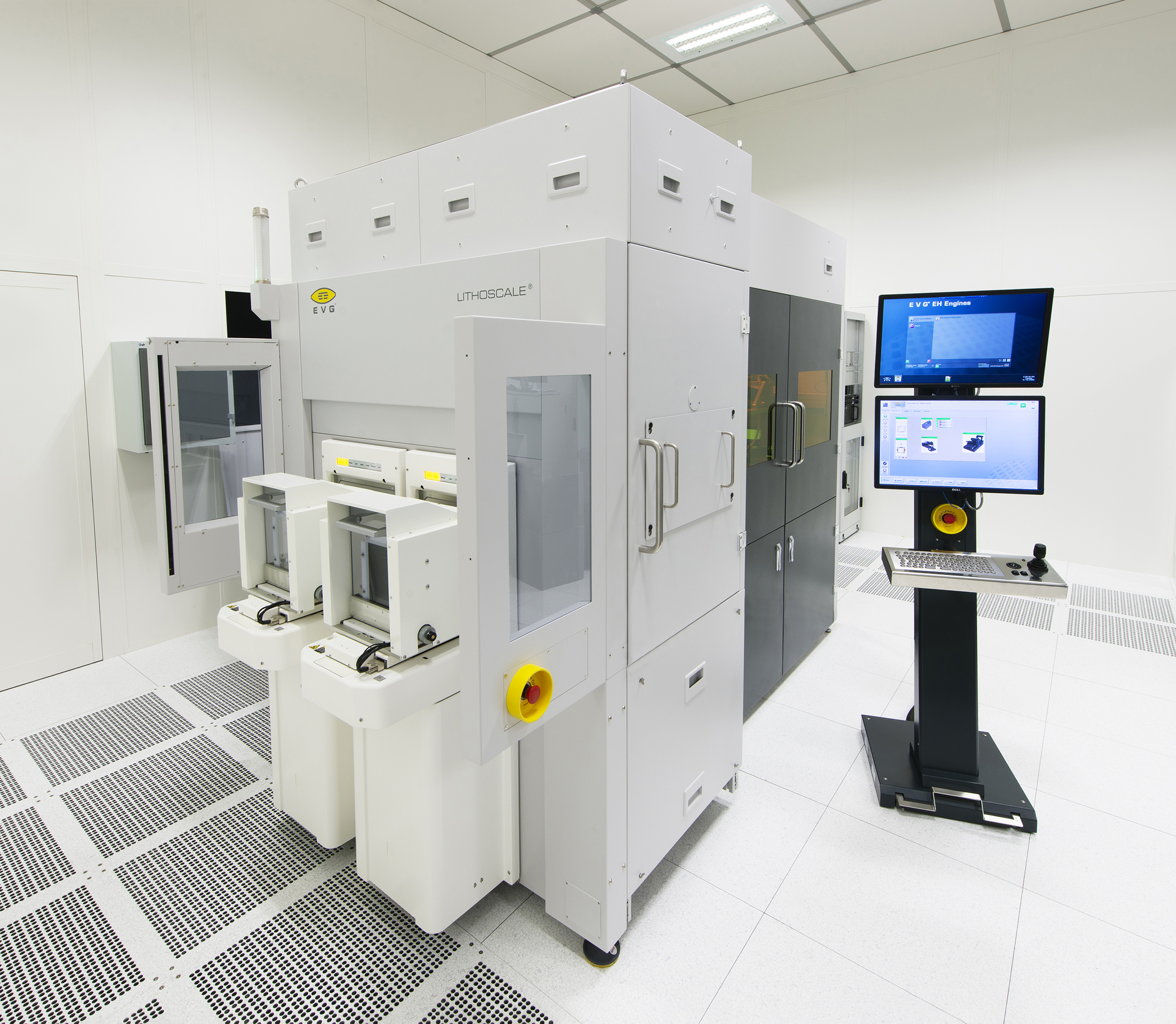
LITHOSCALE® Maskless Exposure Lithography System

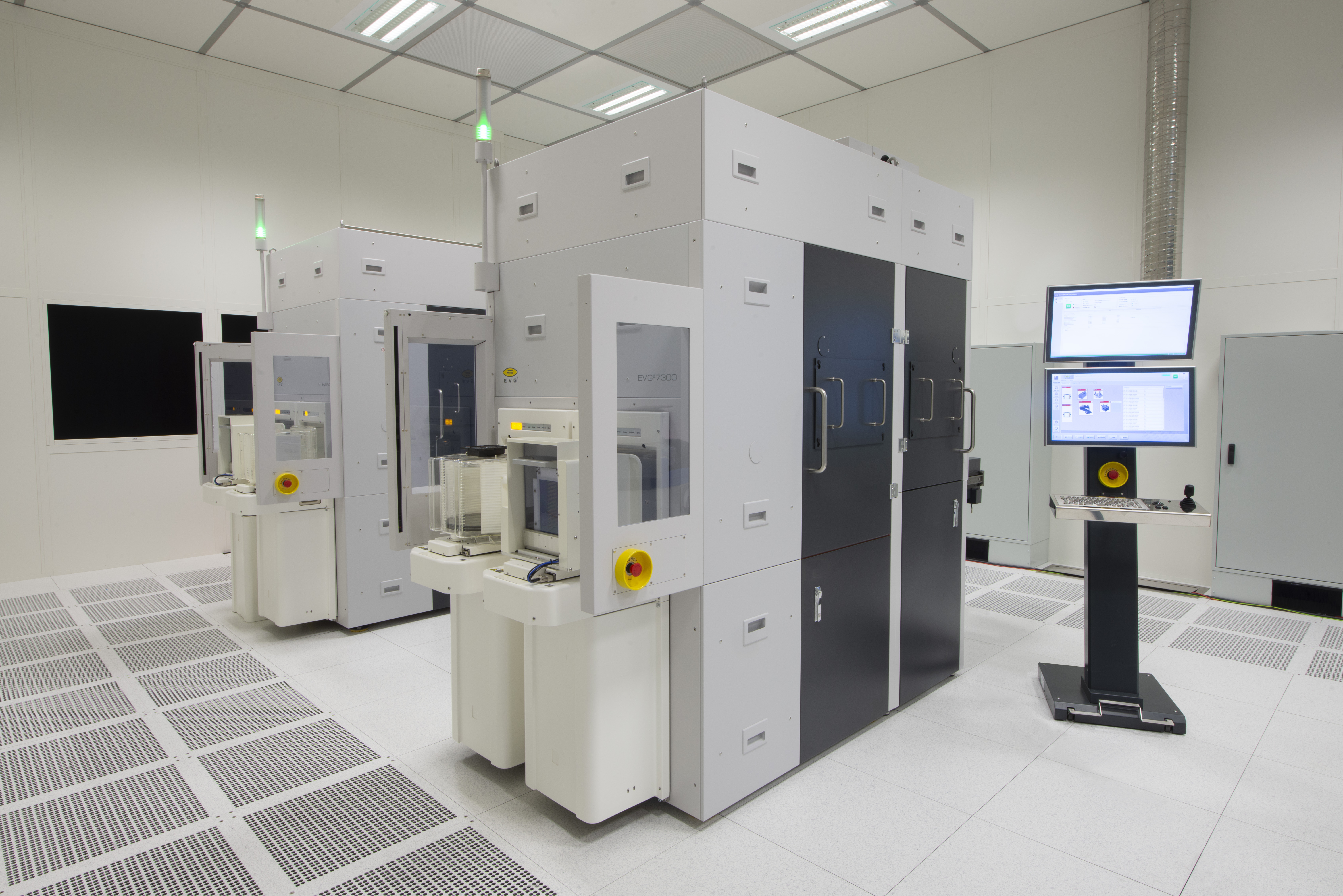
EVG®7300 Multifunctional UV Nanoimprint Lithography System
ST. FLORIAN / GRAZ, Austria, November 13, 2023—EV Group (EVG), a leading supplier of wafer bonding and lithography equipment for the MEMS, nanotechnology and semiconductor markets, and Silicon Austria Labs (SAL), Austria’s leading research center for Electronic Based Systems (EBS), today announced that SAL has received and installed multiple EVG lithography and resist processing systems at its MicroFab R&D cleanroom facility in Villach, Austria. The installations are part of a strengthened collaboration between the two companies to accelerate the development and deployment of advanced optical technologies for heterogeneous integration applications, including wafer-level optics used for micro cameras and micro-mirrors, diffractive optics, and automotive optics used to enable autonomous driving and automotive lighting.
The newly installed EVG systems include the LITHOSCALE® maskless exposure system, the EVG®7300 automated SmartNIL® nanoimprint and wafer-level optics system, as well as multiple complementary resist processing systems. These systems join SAL’s existing installed base of multiple EVG bonding, mask alignment and lithography systems, including the first installation of the next-generation 200-mm version of the EVG®150 automated resist processing system, which provides significantly higher throughput, increased flexibility and smaller tool footprint compared to the previous-generation platform.
In addition, SAL has been working closely with the technology development and application engineering team at EVG’s headquarters, including the NILPhotonics® Competence Center, to leverage EVG’s equipment and process knowhow and develop processes that are transferrable and scalable to high-volume manufacturing.
According to Dr. Mohssen Moridi, Head of Research Division Microsystems at Silicon Austria Labs, “We have recently been immersed in a range of cutting-edge R&D projects spanning meta-optics, integrated photonics, and MEMS, necessitating the use of advanced lithography and bonding tools. Through our valued partnership with EVG, we have gained access to tools of exceptional reliability and precision, paramount for successful R&D endeavors. Notably, the EVG7300 SmartNIL system has emerged as a pivotal tool, enabling the mass production of nanostructures for emerging photonics and MEMS devices. Its applications extend to diverse fields such as smart lighting systems, AR/VR, automotive optics, telecommunication, and quantum technology.”
SAL was among the first customers to receive the new EVG7300 system, which is EVG’s most advanced solution to combine multiple UV-based process capabilities, such as nanoimprint lithography (NIL), lens molding and lens stacking (UV bonding), in a single platform. The EVG7300 was specifically developed to serve advanced R&D and production needs for a wide range of emerging applications involving micro- and nano-patterning as well as functional layer stacking.
EVG’s revolutionary LITHOSCALE maskless exposure system addresses lithography needs for markets and applications that require a high degree of flexibility or product variation. It tackles legacy bottlenecks by combining powerful digital processing that enables real-time data transfer and immediate exposure, high structuring resolution and throughput scalability. It is ideally suited for rapid prototyping, providing fast turnaround and R&D cycle times.
According to Thomas Glinsner, corporate technology director at EV Group, “Silicon Austria Labs is a leading research center for optical miniaturization and heterogeneous integration, and is a strategic partner for EV Group. This latest shipment and installation of our advanced lithography and resist processing systems further strengthens our relationship and supports SAL’s ability to develop future key technologies and apply our leading-edge solutions into real-world industrial applications.”
See EVG at SEMICON Europa
SEMICON Europa attendees interested in learning more about EVG and its suite of wafer bonding, lithography and metrology solutions for heterogeneous integration are invited to visit EVG at booth B1213 (Hall B1) on November 14-17 at the Messe München Convention Center in Munich, Germany.
About Silicon Austria Labs (SAL)
Silicon Austria Labs GmbH (SAL) was founded in 2018 as part of the European Forum Alpbach as a cross-state, non-university center of excellence in the field of electronics-based systems. At its locations in Graz, Villach and Linz, research is conducted on key technologies in the fields of Microsystems, Sensor Systems, Power Electronics, Intelligent Wireless Systems and Embedded Systems. SAL brings together key players from industry and science and thus valuable expertise and know-how, and conducts cooperative, application-oriented research along the value chain. The aim is to accelerate the value creation process from idea to innovation - with excellent research and economic benefits. Owners are the Republic (50.1%), the Provinces of Styria and Carinthia (10% each), the Province of Upper Austria (4.95%) and the Professional Association for the Electrical and Electronics Industry (24.95%). More information about SAL is available at https://silicon-austria-labs.com/.
About EV Group (EVG)
EV Group (EVG) is a leading supplier of equipment and process solutions for the manufacture of semiconductors, microelectromechanical systems (MEMS), compound semiconductors, power devices and nanotechnology devices. Key products include wafer bonding, thin-wafer processing, lithography/nanoimprint lithography (NIL) and metrology equipment, as well as photoresist coaters, cleaners and inspection systems. Founded in 1980, EV Group services and supports an elaborate network of global customers and partners all over the world. More information about EVG is available at www.EVGroup.com.
Silicon Austria Labs Contact:
Isabella Preuer
Head of Communications & PR
Silicon Austria Labs
Tel: +43 664 832 97 73
E-mail: press@silicon-austria.com
EV Group Contacts:
Clemens Schütte
Director, Marketing and Communications
EV Group
Tel: +43 7712 5311 0
E-mail: Marketing@EVGroup.com
David Moreno
Principal
Open Sky Communications
Tel: +1.415.519.3915
E-mail: dmoreno@openskypr.com