DI Erich Thallner Strasse 1
4782 St. Florian am Inn
Austria
Press Center
27.08.2024
EV Group Highlights 3D Integration Process Solutions at SEMICON Taiwan 2024
11.07.2024
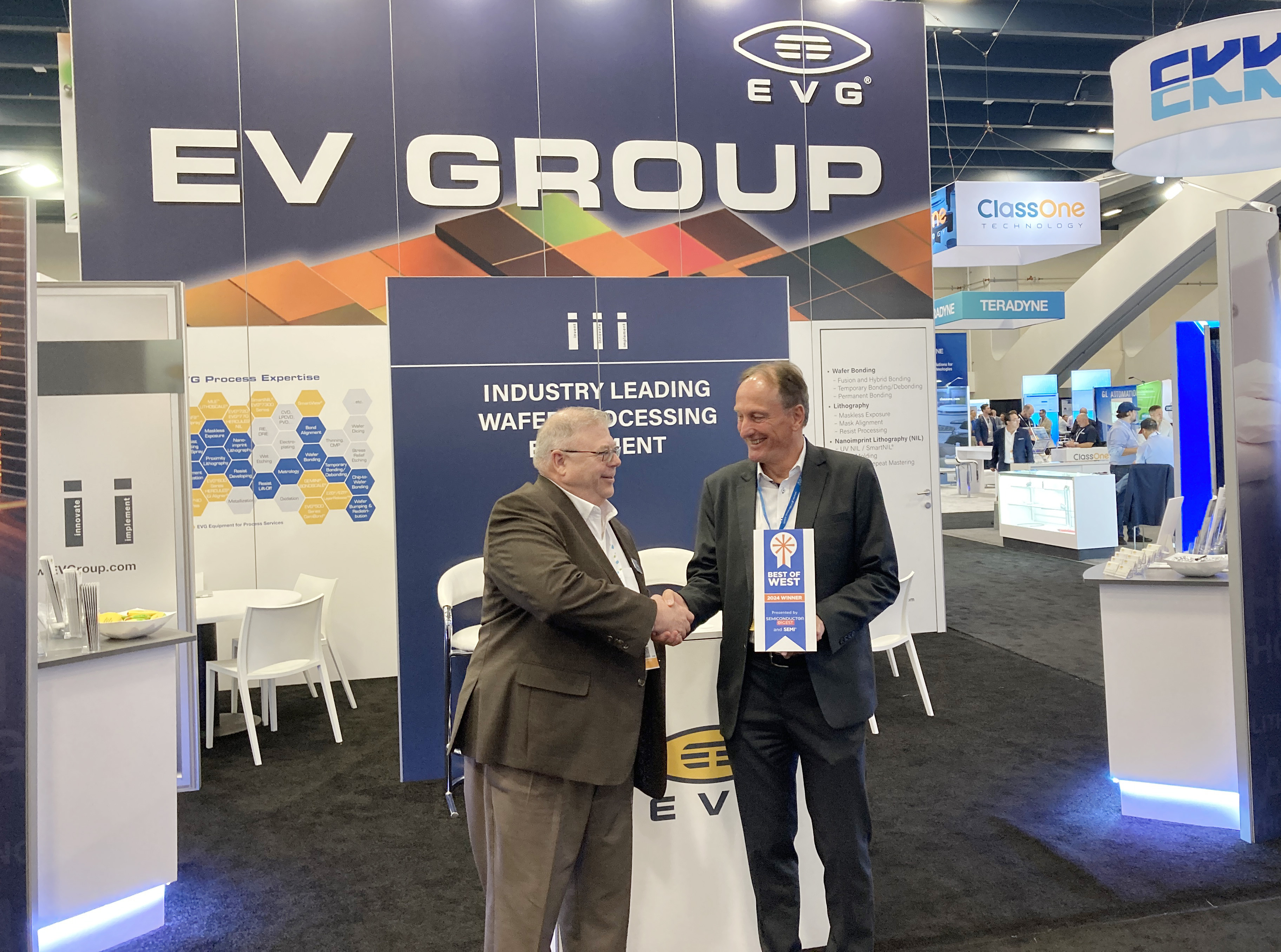
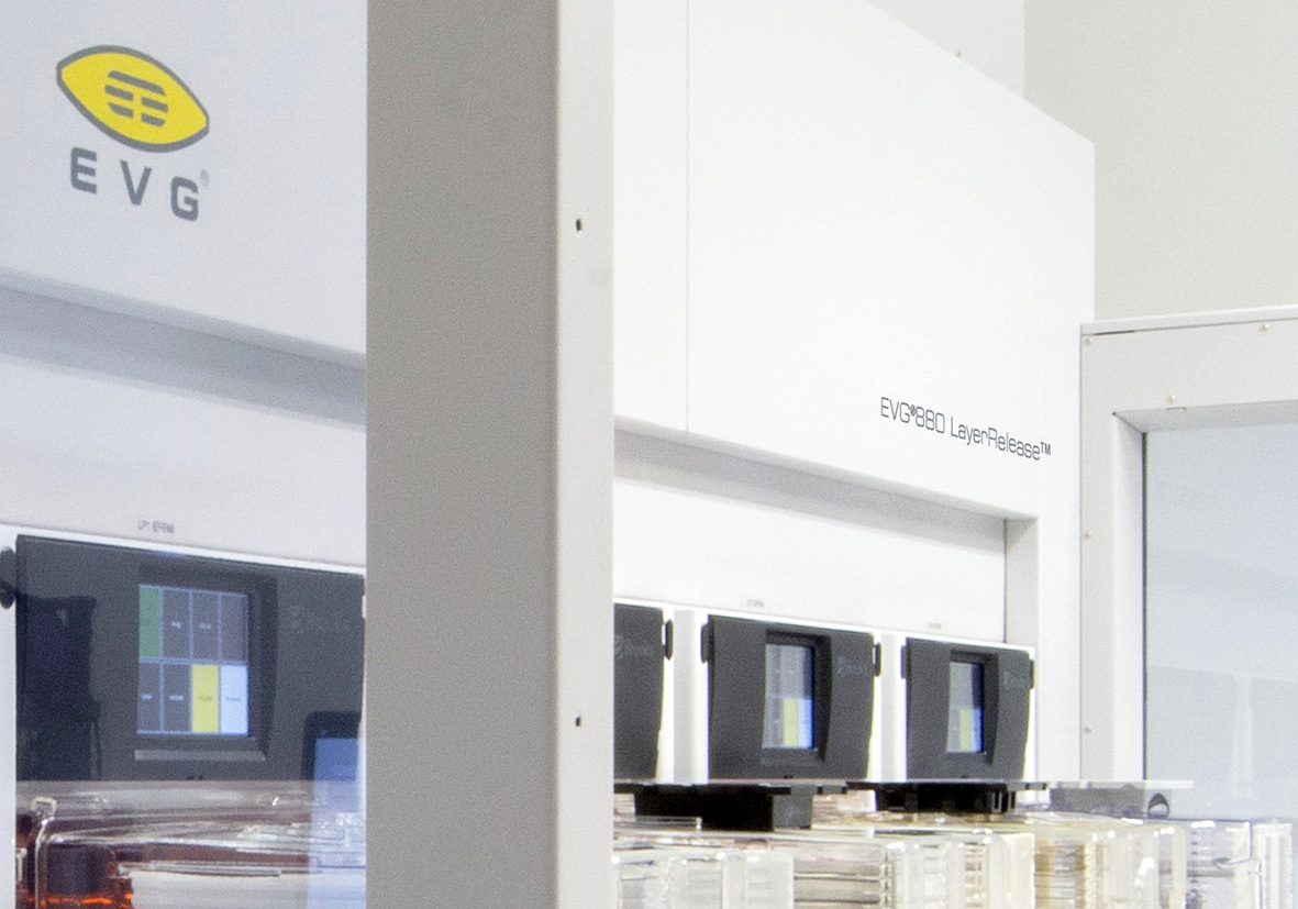
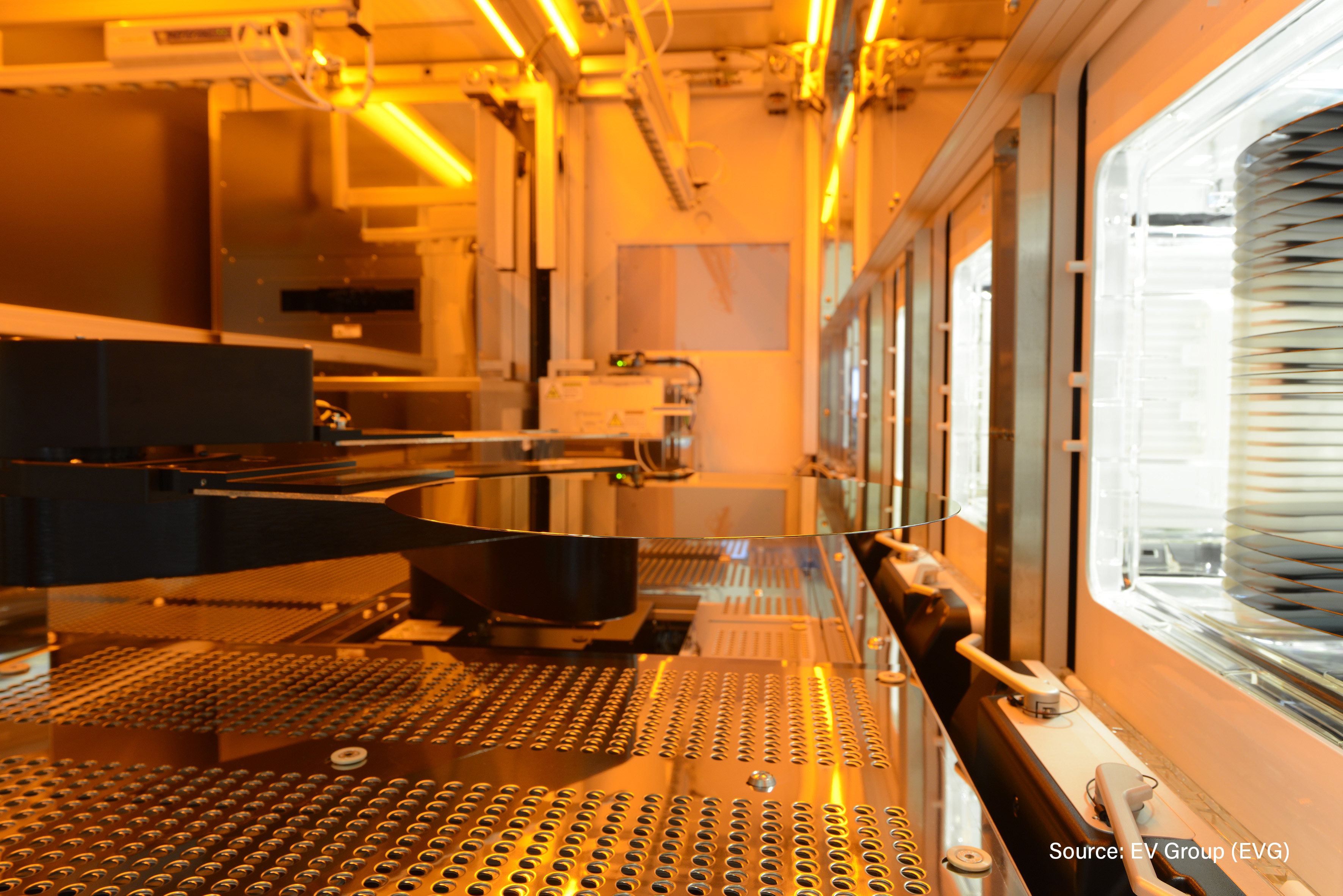
EV Group’s EVG®880 LayerRelease™ System Wins 2024 Best of West Award
01.07.2024
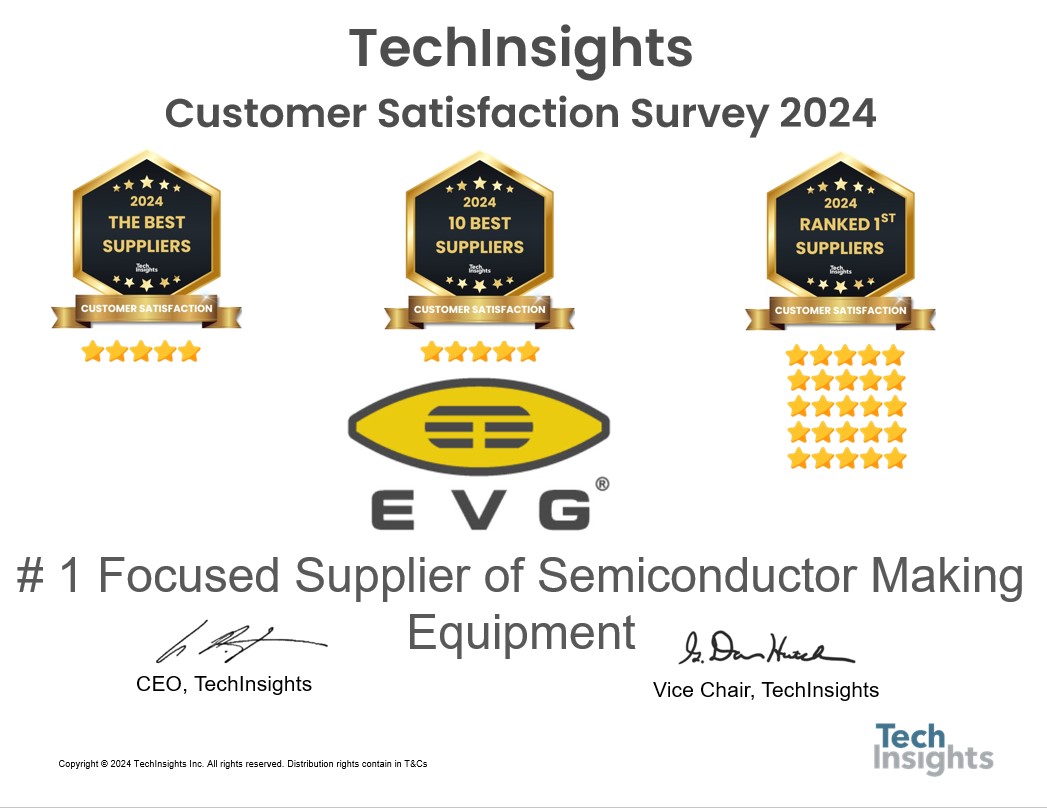
EV Group Tops Customer Rankings With 12th Consecutive Triple Crown Win in TechInsights 2024 Customer Satisfaction Survey
18.06.2024
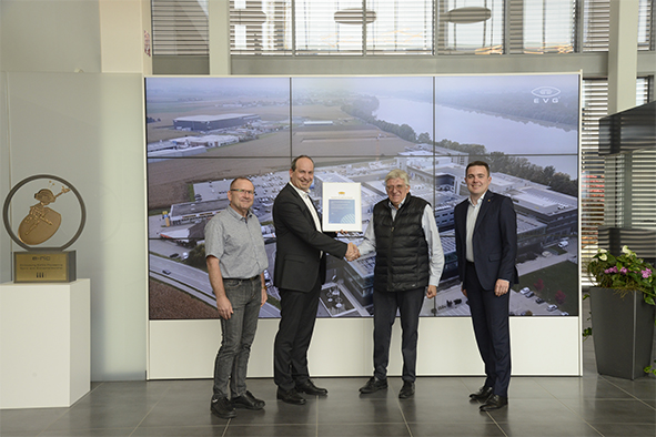
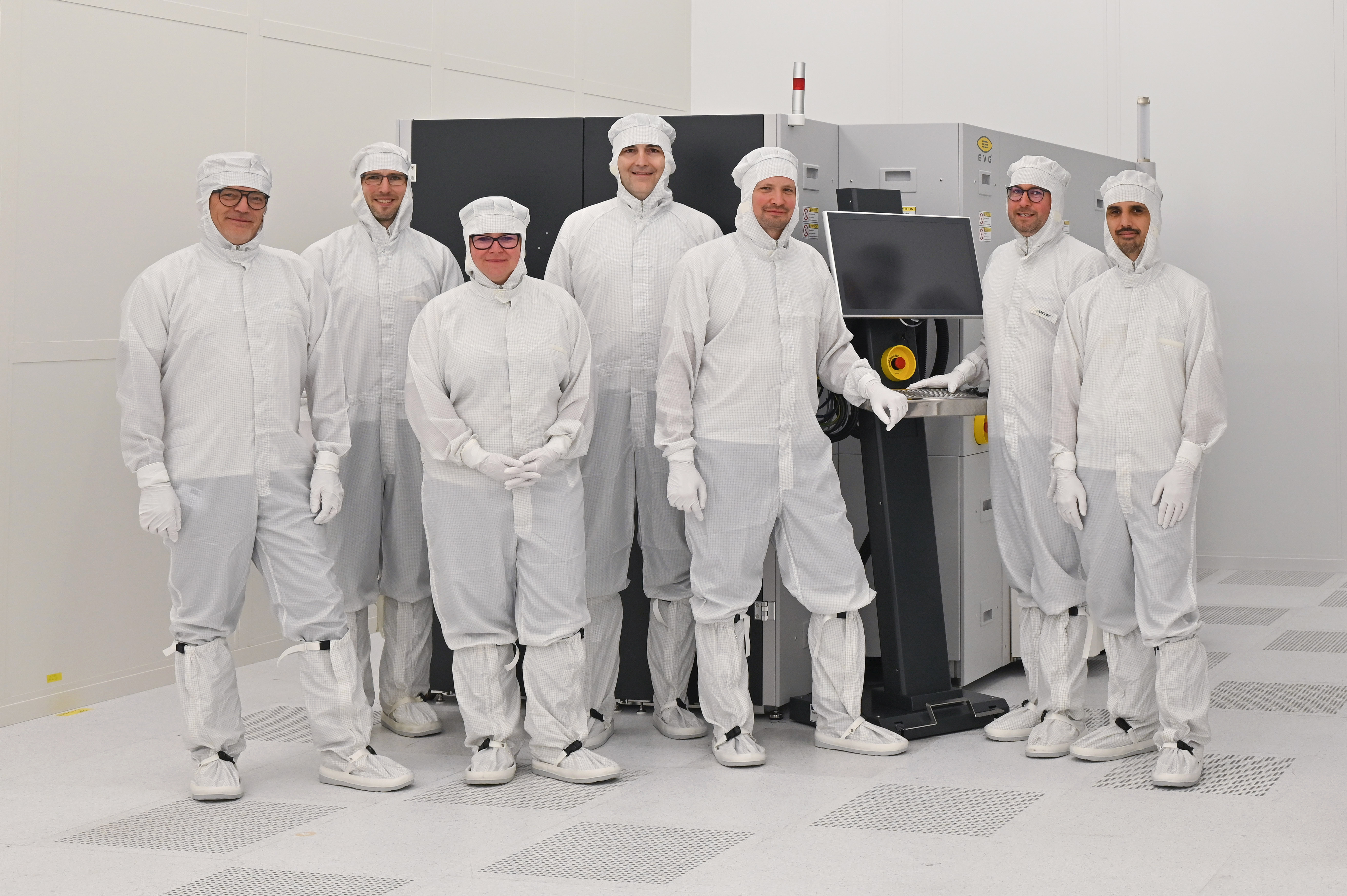
KYOCERA Fineceramics Europe GmbH wins supplier excellence award from EV Group (EVG)
13.06.2024
EV集团与弗劳恩霍夫可靠性和微集成研究所扩大在量子计算应用晶圆键合领域的合作
28.05.2024
全新 EVG®880 LayerRelease™ 离型层系统将半导体层转移技术产量提高一倍
15.05.2024
EV Group Hybrid Bonding, Maskless Lithography and Layer Transfer Solutions for Heterogeneous Integration to be Highlighted at ECTC 2024
03.04.2024