DI Erich Thallner Strasse 1
4782 St. Florian am Inn
Austria
Press Center

26.05.2025
EV Group Brings Digital Lithography to Heterogeneous Integration HVM Applications with LITHOSCALE® XT
19.05.2025
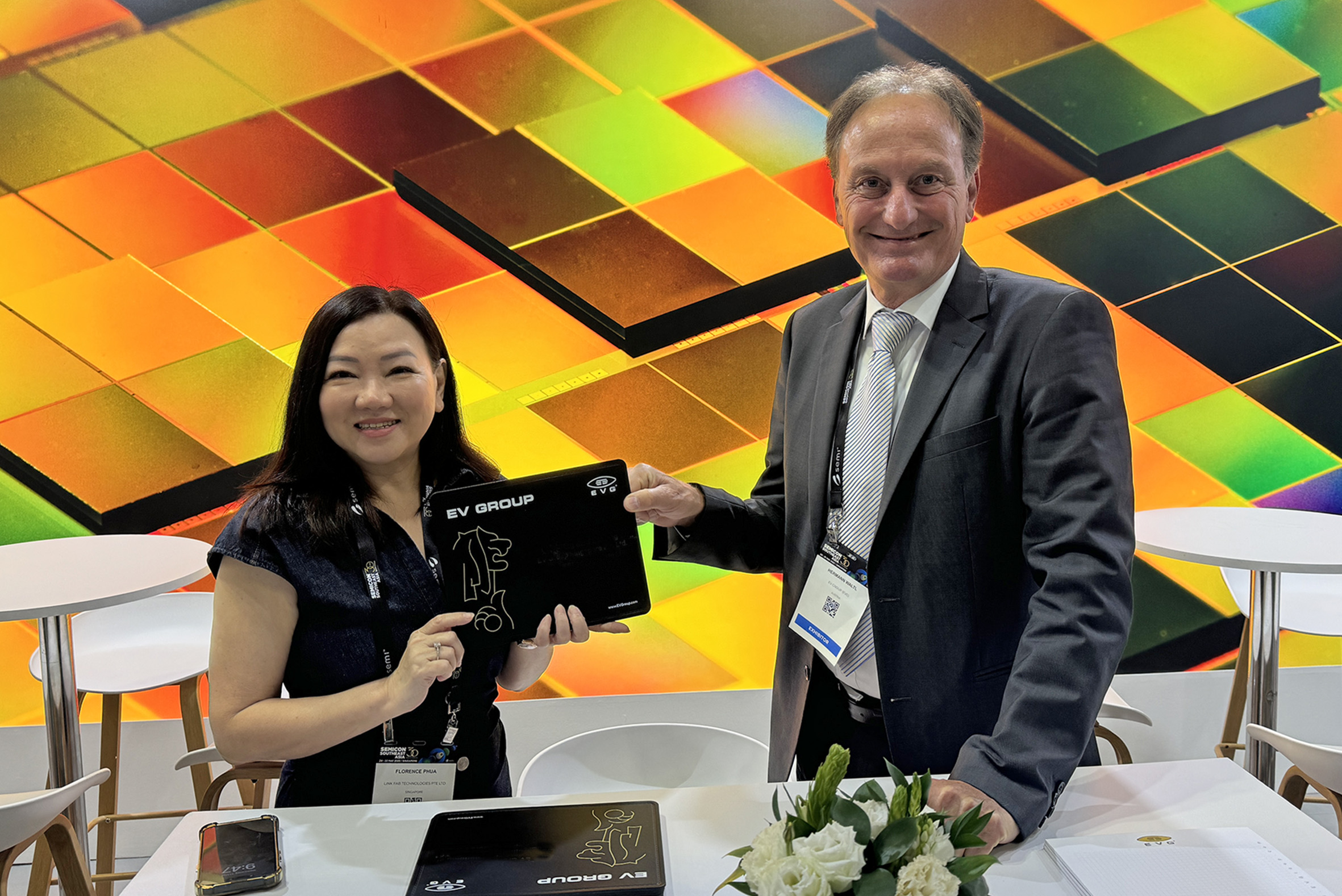
EV Group Forms Subsidiary in Singapore to Strengthen Local Customer Support
14.05.2025
EV Group Hybrid Bonding, Maskless Lithography and Layer Transfer Solutions for Heterogeneous Integration to be Highlighted at ECTC 2025
30.04.2025
EV Group Appoints Dr. Thomas Uhrmann Vice President of Sales
26.03.2025
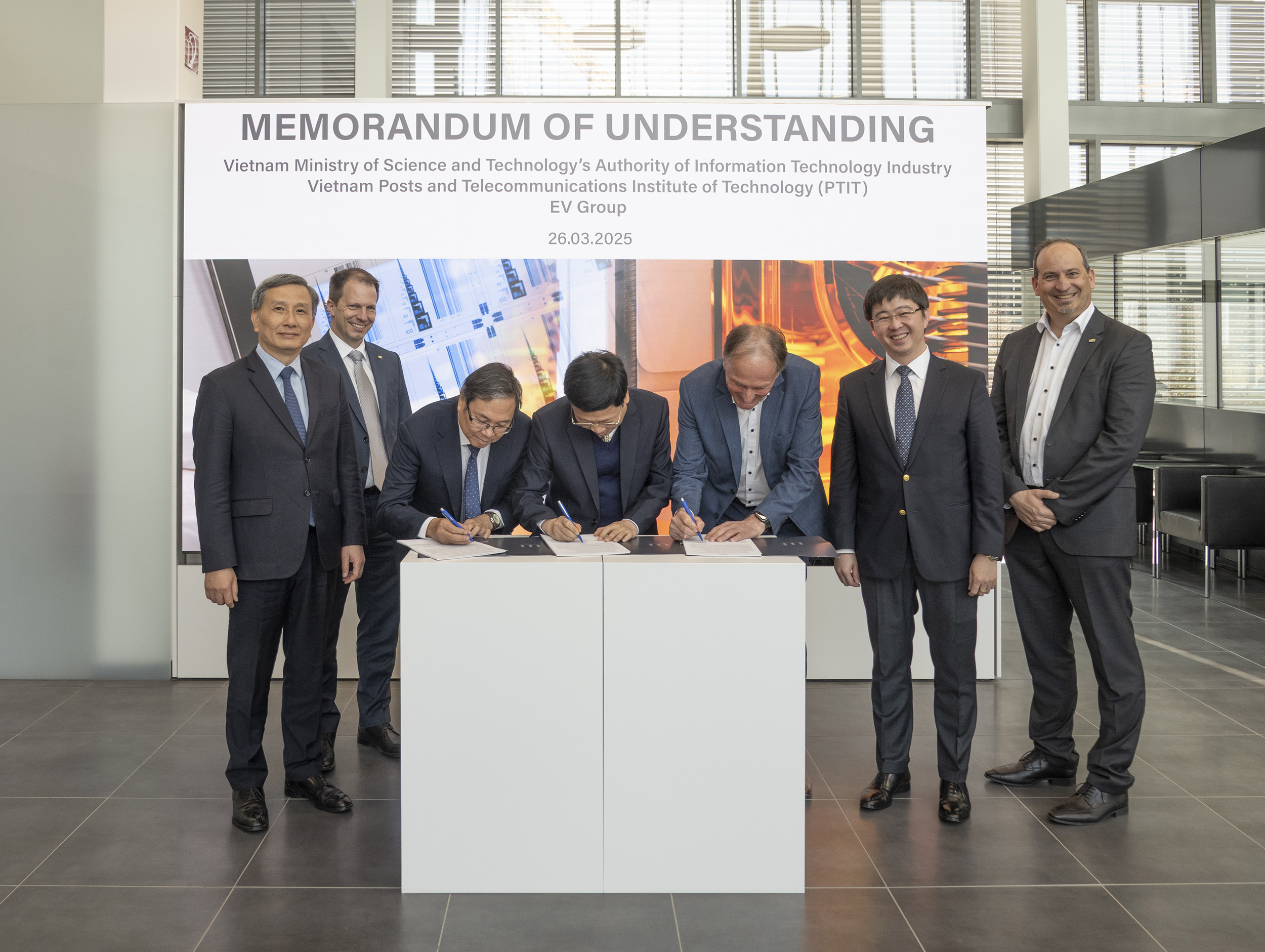
EV Group, Vietnam’s Authority of Information Technology Industry and PTIT Sign Memorandum of Understanding to Advance Vietnam's Semiconductor Capabilities
18.03.2025
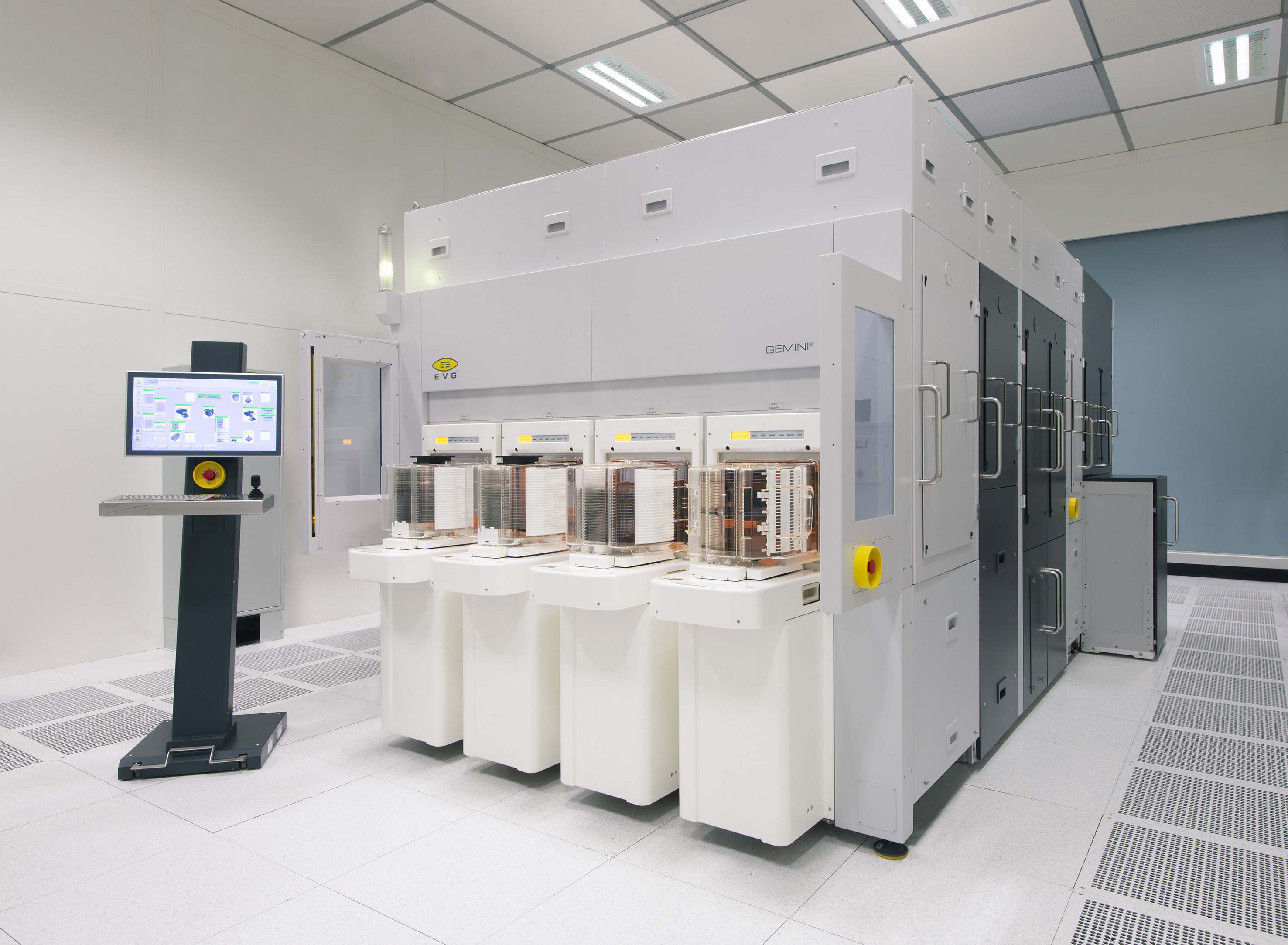
EV集团推出面向300毫米晶圆的下一代GEMINI®全自动生产晶圆键合系统,推动MEMS制造升级

18.02.2025
EV Group Highlights Revolutionary Temporary Wafer Bonding and Debonding Solution for HBM and 3D DRAM at SEMICON Korea
24.10.2024