DI Erich Thallner Strasse 1
4782 St. Florian am Inn
Austria
ZH
中文 (ZH)
Press Center
22.01.2020
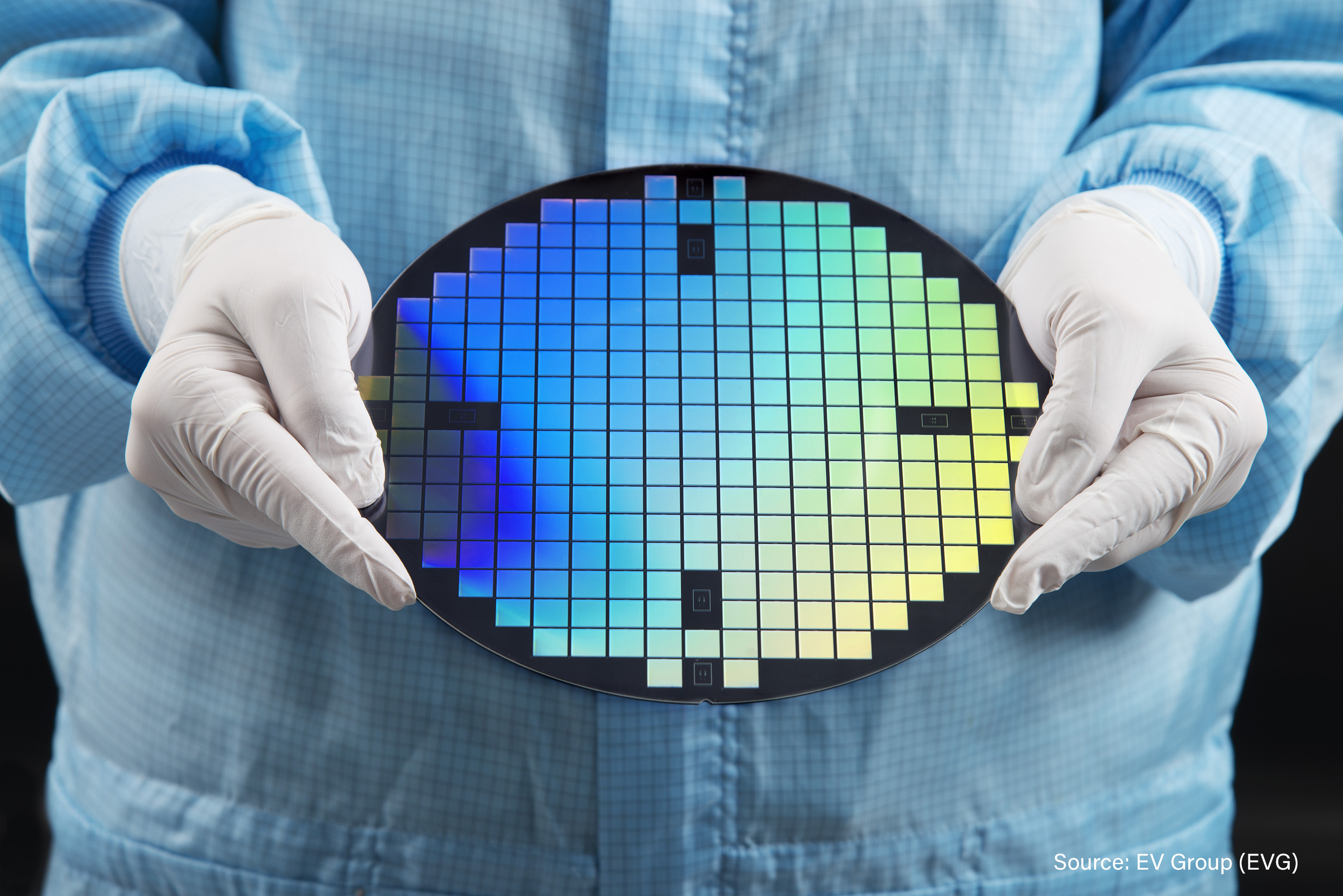
EV Group and INKRON Partner on High Refractive Index Materials and Nanoimprint Lithography Development for Next-Generation Optical Devices
阅读更多
12.11.2019
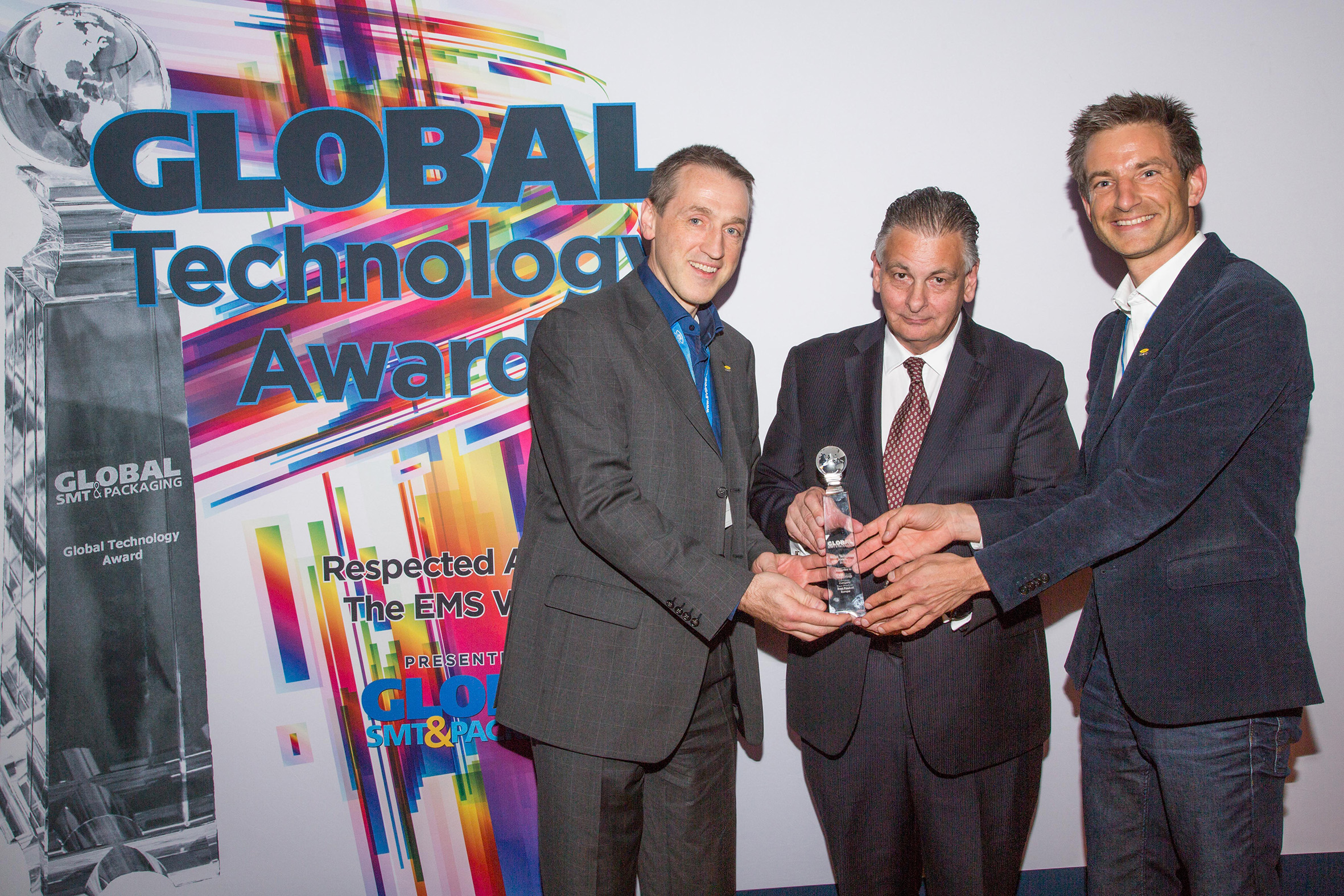
EV Group Wins Global Technology Award for MLE™ Maskless Exposure Technology at productronica and SEMICON Europa
阅读更多
11.11.2019
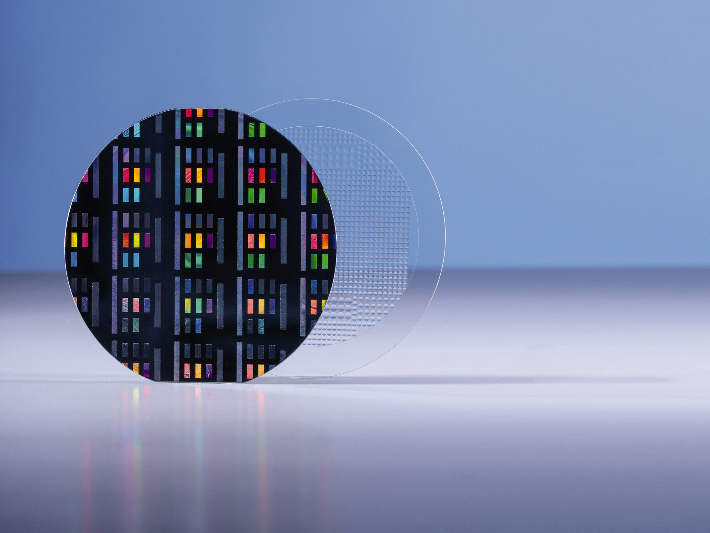
EV Group and DELO Partner to Expand Materials and Process Capabilities For Wafer-Level Optics and Nanoimprint Lithography
阅读更多

09.10.2019
APPLAUSE – an ECSEL Joint Undertaking project – focuses on developing advanced packaging for photonics, optics and electronics for low cost manufacturing
阅读更多
27.08.2019
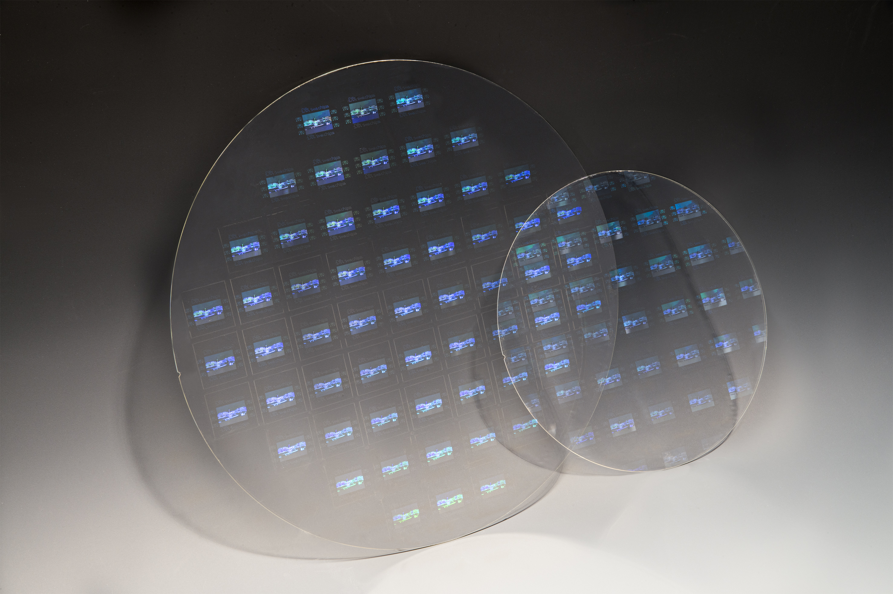
EV集团和肖特携手合作,证明300-MM光刻/纳米压印技术在大体积增强现实/混合现实玻璃制造中已就绪
阅读更多

27.08.2019
EV集团利用新型无掩膜曝光(MLE)重塑光刻技术
阅读更多

08.07.2019
EV Group Earns Exceptional Seventh Consecutive Triple Crown Win in VLSIresearch 2019 Customer Satisfaction Survey
阅读更多
24.06.2019
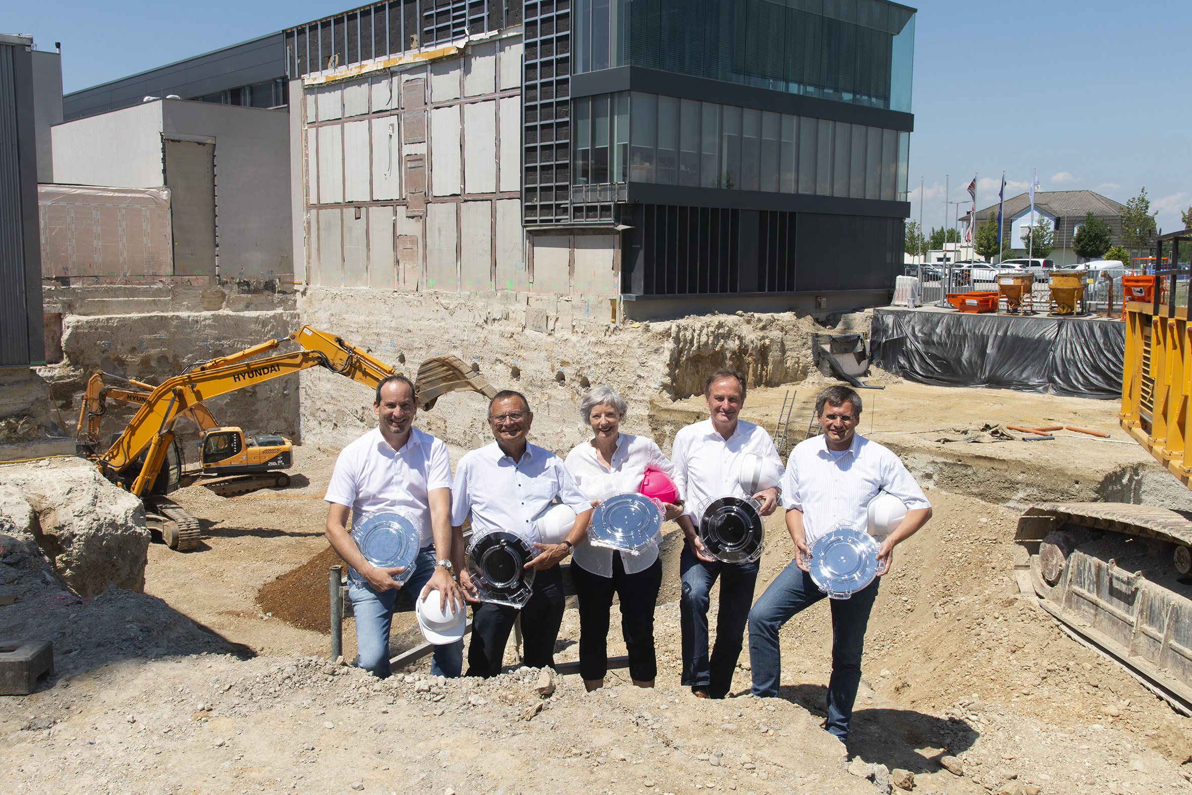
EV Group Invests 30 Million Euros for Capacity Expansion at Corporate Headquarters in Austria
阅读更多