DI Erich Thallner Strasse 1
4782 St. Florian am Inn
Austria
EN
English (EN)
Menu
- Products
-
Technologies
- IR LayerRelease™ Technology
- MLE™ - Maskless Exposure Technology
- Nanoimprint Lithography (NIL) - SmartNIL®
- Wafer Level Optics
- Optical Lithography
- Resist Processing Technology
- Temporary Bonding and Debonding
- Eutectic Bonding
- Transient Liquid Phase (TLP) Bonding
- Anodic Bonding
- Metal Diffusion Bonding
- Hybrid and Fusion Bonding
- Die-to-Wafer Fusion and Hybrid Bonding
- ComBond® Technology
- Metrology
- Company
- Careers
Search
Press Center
22.01.2020
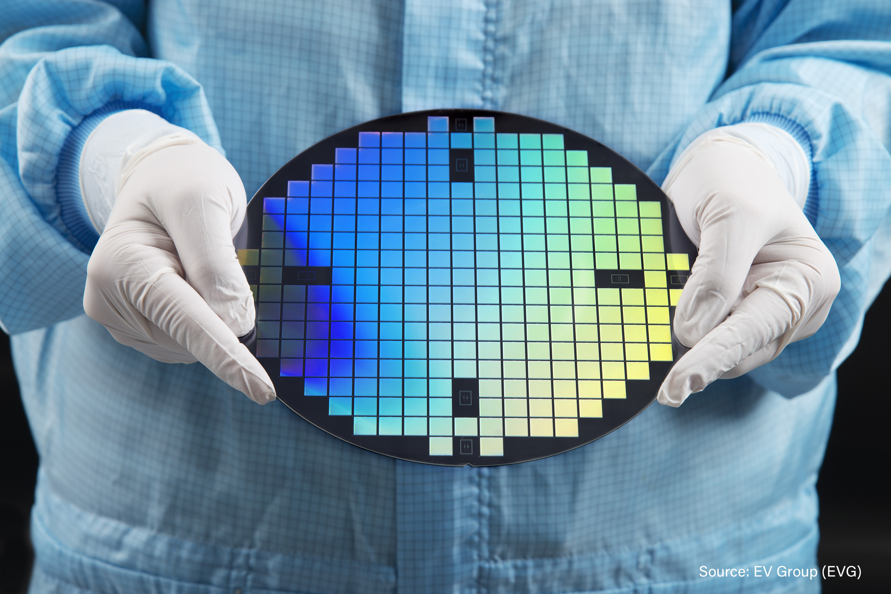
EV Group and INKRON Partner on High Refractive Index Materials and Nanoimprint Lithography Development for Next-Generation Optical Devices
Read more
12.11.2019
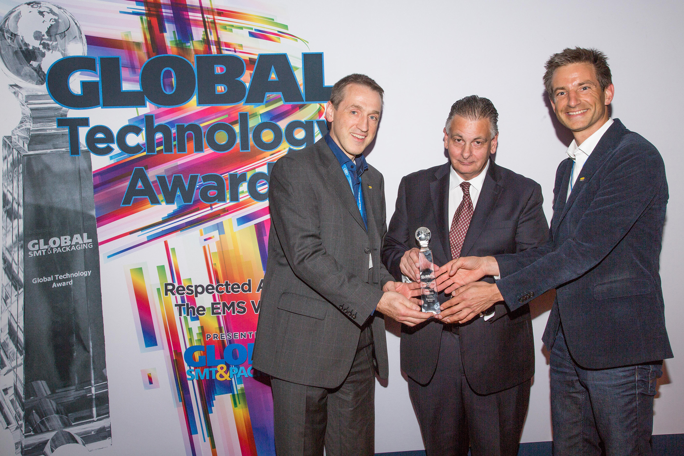
EV Group Wins Global Technology Award for MLE™ Maskless Exposure Technology at productronica and SEMICON Europa
Read more

11.11.2019
EV Group and DELO Partner to Expand Materials and Process Capabilities For Wafer-Level Optics and Nanoimprint Lithography
Read more

09.10.2019
APPLAUSE – an ECSEL Joint Undertaking project – focuses on developing advanced packaging for photonics, optics and electronics for low cost manufacturing
Read more
28.08.2019
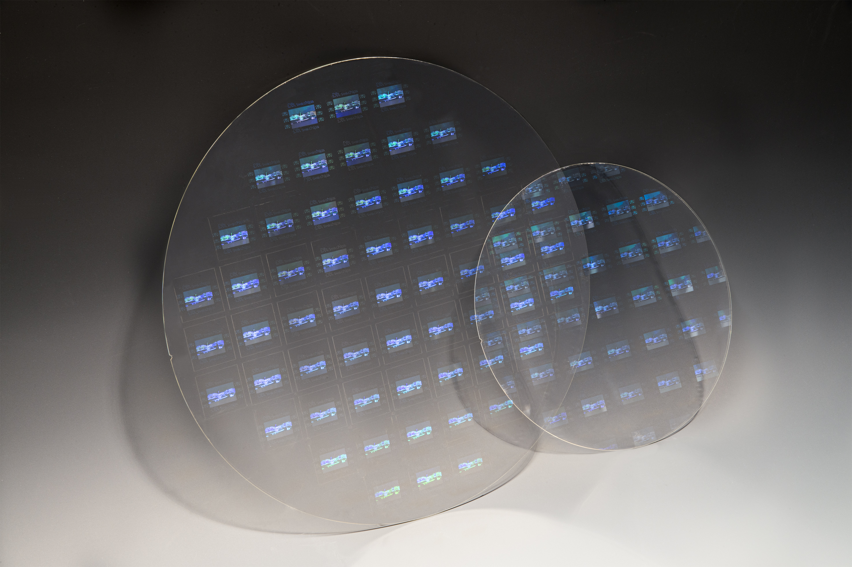
EV Group and SCHOTT Partner to Demonstrate Readiness of 300-mm Nanoimprint Lithography for High-Volume Augmented/Mixed Reality Glass Manufacturing
Read more

08.07.2019
EV Group Earns Exceptional Seventh Consecutive Triple Crown Win in VLSIresearch 2019 Customer Satisfaction Survey
Read more

02.07.2019
EV Group Revolutionizes Lithography with New Maskless Exposure Technology
Read more
24.06.2019
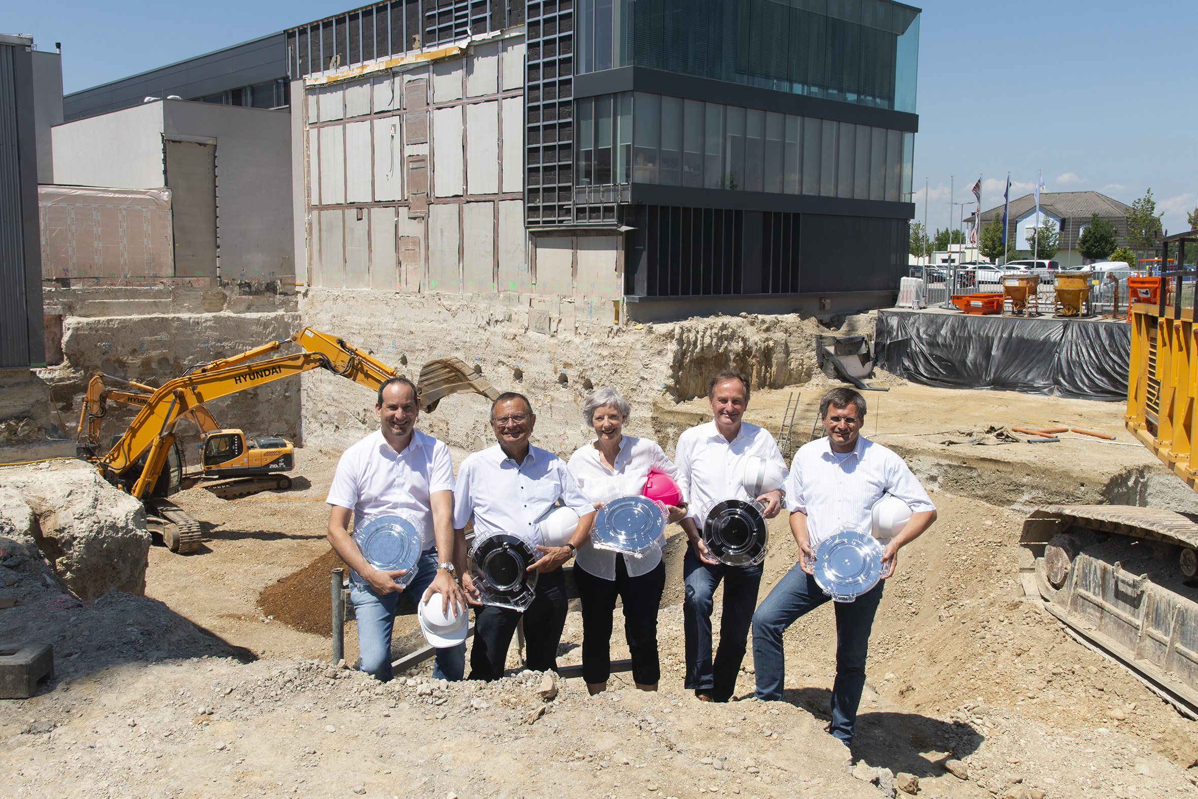
EV Group Invests 30 Million Euros for Capacity Expansion at Corporate Headquarters in Austria
Read more
EV Group - Press contact
Phone