Die-to-Wafer Fusion and Hybrid Bonding
Collective and direct-placement die-to-wafer bonding
Introduction
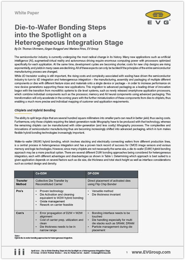
Wafer-to-wafer hybrid bonding, which involves stacking and electrically connecting wafers from different production lines, is a central process in heterogeneous integration and has a proven track record of success for CMOS image sensors and various memory and logic technologies. However, since many chiplets are not necessarily the same size, a die-to-wafer hybrid bonding approach may be a more practical option. There are several different die-to-wafer bonding approaches being considered for heterogeneous integration – Collective D2W as well as direct placement D2W bonding – each delivering individual pros and cons as shown in the table below:
| Co-D2W | DP-D2W | |
|---|---|---|
| Transfer Method | Collective Die Transfer by Reconstituted Carrier | Direct placement of activated dies using Flip Chip Bonder |
| Pros | - Proven technology- Die Activation and cleaning equivalent to W2W hybrid bonding- Oxide management- Rework on carrier feasible | - Versatile method- Die thickness invariant |
| Cons | - Error propagation of D2W + W2W alignment- Cost of carrier prep, utilization and clean- Die thickness needs to be in narrow range | - Bonding interface needs to be touched- Die handling especially for multi die stacks such as SRAM, DRAM- Particle management during die placement |
Collective Die-to-Wafer Bonding
One hybrid die-to-wafer bonding method that has already been implemented in limited volume production for the past few years for applications such as silicon photonics is collective die-to-wafer (Co-D2W) bonding. In Co-D2W bonding, multiple dies are transferred to the final wafer in a single process step. The manufacturing flow for the Co-D2W bonding process is shown in the figure below and consists of four major segments: carrier preparation, carrier population, wafer bonding (temporary and permanent) and carrier separation.

Direct Placement Die-to-Wafer Bonding
Another hybrid die-to-wafer bonding approach that is currently being evaluated for heterogeneous integration applications is direct placement die-to-wafer (DP-D2W) bonding whereby the dies are transferred to the final wafer individually using a pick-and-place flip-chip bonder. The Figure below shows the manufacturing flow for the DP-D2W bonding process, which costs of three major segments: carrier population, die clean and activation, and direct placement flip chip.

Accelerating Technology Development with EVG's Heterogeneous Integration Competence Center™
To address these challenges, EVG established the Heterogeneous Integration Competence Center™ (HICC), which assists customers in leveraging EVG process solutions and expertise to enable new and enhanced products and applications driven by advances in system integration and packaging. The basic idea for the foundation of the HICC is to make the barriers for development as low as possible to customers and to offer EVG as an incubator for new ideas. Through the HICC, EVG can assist in accelerating technology development, minimizing risk, and developing differentiating technologies and products through heterogeneous integration and advanced packaging all while guaranteeing the highest IP protection standards that are required for working on pre-release products.
TEM cross section of hybrid bonded dies using collective D2W bonding (Co-D2W)
")
Events

ICEPT 2024
Listen to our presentation "Metal/Dielectric Hybrid Bonding for Heterogenous Integration Applications" held by Dr. Viorel Dragoi.

SEMICON Taiwan 2024
Visit our booth #L0316 & listen to our talks:
"Disruptive 3D Integration Technologies for Advanced Stacked Systems" at the HIGS Summit and "Maskless Patterning Solution for multi-functional chiplets in advanced System-in-Package (SiP)" at the TechXSpot.

Talk to our EVG technology experts!
Questions?
Questions about our technologies?
Contact the EVG experts
Download
EVG® Whitepaper
Die-to-Wafer Bonding