DI Erich Thallner Strasse 1
4782 St. Florian am Inn
Austria
EV Group Breaks Speed and Accuracy Barrier in Mask Alignment Lithography for Semiconductor Advanced Packaging
New IQ Aligner NT achieves double throughput and alignment accuracy over previous-generation platform; opens up new applications for EVG lithography solutions

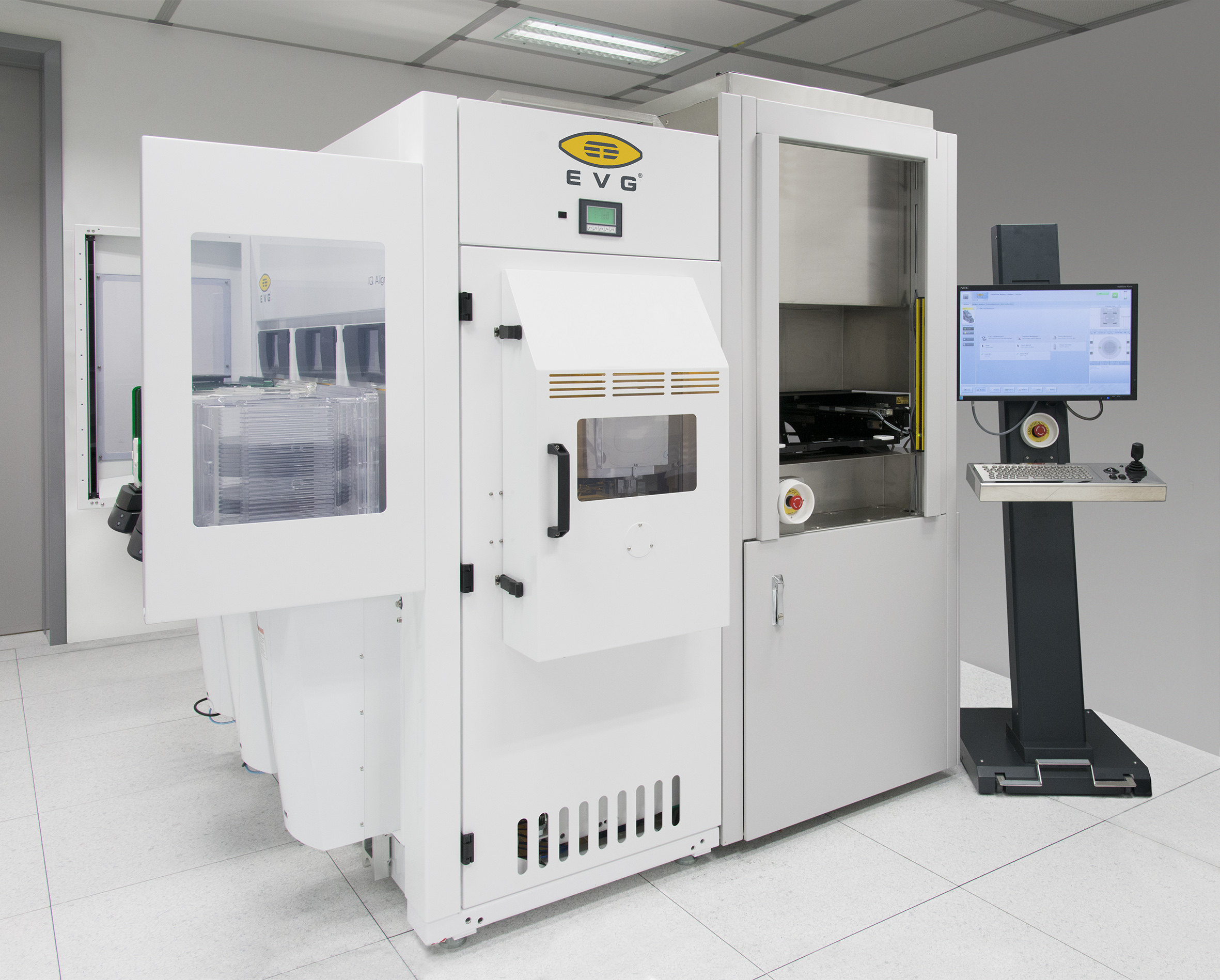
IQ Aligner®NT Automated Mask Alignment System
ST. FLORIAN, Austria, March 8, 2017 — EV Group (EVG), a leading supplier of wafer bonding and lithography equipment for the MEMS, nanotechnology and semiconductor markets, today unveiled the IQ Aligner NT-its latest and most advanced automated mask alignment system for high-volume advanced packaging applications. Featuring high-intensity and high-uniformity exposure optics, new wafer handling hardware, full 200-mm and 300-mm wafer coverage that enables global multi-point alignment, and optimized tool software, the new IQ Aligner NT provides a 2X increase in throughput and 2X improvement in alignment accuracy over EVG's previous-generation IQ Aligner. The system surpasses the most demanding requirements for wafer bump and other back-end lithography applications while providing up to 30 percent lower cost of ownership compared to competing systems.
The IQ Aligner NT is ideally suited for a variety of advanced packaging types, including Wafer-level Chip Scale Packaging (WLCSP), Fan-out Wafer Level Packaging (FOWLP), 3D-IC/Through-silicon Via (TSV), 2.5D Interposers, and Flip Chip.
New lithography capabilities needed
Semiconductor advanced packaging is continually evolving to enable new types of devices with increasing functionality at a lower cost per function. As a result, new developments in lithography are now required to address the unique needs of the advanced packaging market. These needs include:
- Extremely tight alignment accuracy
- Managing wafer warpage and addressing dimensional mismatch of wafer and mask layout to achieve optimized overlay
- Sufficient exposure of the thicker resists and dielectric layers found in back-end processing
- Higher resolution to address shrinking bumps and interconnects due to device scaling
- At the same time, all of these needs must be met in a highly cost-effective and high-productivity lithography tool platform.
"Leveraging more than three decades of experience in lithography, EVG has pushed the envelope of mask alignment technology to new boundaries with our new IQ Aligner NT," stated Paul Lindner, executive technology director at EV Group. "This latest addition to our suite of lithography solutions provides unprecedented levels of throughput, accuracy and cost-of-ownership performance, which in turn has opened up a variety of new market opportunities for EVG. We look forward to working closely with customers to meet their critical advanced packaging lithography needs."
The IQ Aligner NT incorporates a variety of improvements to achieve industry-leading mask alignment performance for advanced packaging lithography:
- High-power optics provides a 3X increase in illumination intensity compared to EVG's previous-generation IQ Aligner, making it ideal for exposing thick resists and other films associated with processing bumps, pillars and other high-topography features
- Full clearfield mask movement over 300-mm substrates, which offers the highest process compatibility and flexibility in dark field mask alignment and pattern positioning
- Dual substrate size concept eliminates the need for any retooling effort, providing a quick and easy on-the-fly bridge tool for two different wafer sizes
- Fully automated as well as semi-automated/manual wafer loading operation is supported for maximum flexibility
- Latest EVG CIMFramework system software based on the latest fab software standards and protocols
Unsurpassed accuracy and productivity performance
Combining state-of-the-art optical and mechanical engineering with optimized tool software, the IQ Aligner NT provides a two-fold increase in throughput (>200 wph for first print, >160 wph for top side alignment) as well as a two-fold improvement in alignment accuracy (250nm 3-sigma). As a result of the tighter alignment specification, customers can also realize improved yields for high-end and high-bandwidth packaging products.
More information on the new IQ Aligner NT automated mask alignment system can be found here.
In addition, EVG will showcase the IQ Aligner NT at the SEMICON China exhibition being held March 14-16 at the Shanghai New International Expo Centre in Shanghai, China. Attendees interested in learning more about the IQ Aligner NT as well as EVG's suite of lithography and wafer bonding solutions for advanced packaging are invited to visit the company's booth #4663.
About EV Group (EVG)
EV Group (EVG) is a leading supplier of equipment and process solutions for the manufacture of semiconductors, microelectromechanical systems (MEMS), compound semiconductors, power devices and nanotechnology devices. Key products include wafer bonding, thin-wafer processing, lithography/nanoimprint lithography (NIL) and metrology equipment, as well as photoresist coaters, cleaners and inspection systems. Founded in 1980, EV Group services and supports an elaborate network of global customers and partners all over the world. More information about EVG is available at www.EVGroup.com.
Contacts:
Clemens Schütte
Director, Marketing and Communications
EV Group
Tel: +43 7712 5311 0
E-mail: Marketing@EVGroup.com
David Moreno
Principal
Open Sky Communications
Tel: +1.415.519.3915
E-mail: dmoreno@openskypr.com