DI Erich Thallner Strasse 1
4782 St. Florian am Inn
Austria
- Products
- Technologies
- IR Laser Cleave Technology
- MLE™ - Maskless Exposure Technology
- Nanoimprint Lithography (NIL) - SmartNIL®
- Wafer Level Optics
- Optical Lithography
- Resist Processing Technology
- Temporary Bonding and Debonding
- Eutectic Bonding
- Transient Liquid Phase (TLP) Bonding
- Anodic Bonding
- Metal Diffusion Bonding
- Fusion and Hybrid Bonding
- Die-to-Wafer Fusion and Hybrid Bonding
- ComBond® Technology
- Metrology
- Company
- Careers
EV Group Revolutionizes Lithography with New Maskless Exposure Technology
EVG’s new MLE™ technology provides unsurpassed flexibility, scalability and cost-of-ownership benefits compared to existing high-volume-manufacturing lithography methods

EVG MLE™ (Maskless Exposure) technology

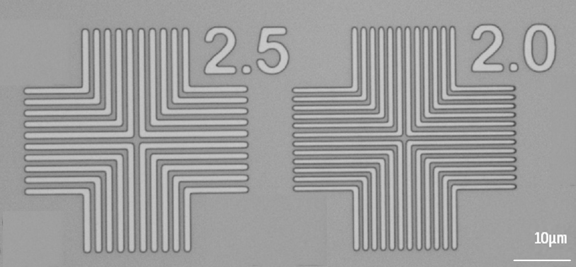
MLE™ exposure in high resolution AZ MIR 701 positive tone photoresist

MLE™ exposure in 50 µm thick layer JSR THB 151N negative tone resist

MLE™ exposure in 600 µm thick SU8

Individual die annotation using MLE™ technology
ST. FLORIAN, Austria, July 2, 2019 — EV Group (EVG), a leading supplier of wafer bonding and lithography equipment for the MEMS, nanotechnology and semiconductor markets, today unveiled MLE™ (Maskless Exposure), a revolutionary next-generation lithography technology developed to address future back-end lithography needs for advanced packaging, MEMS, biomedical and high-density printed circuit board (PCB) applications. The world’s first highly scalable maskless lithography technology for high-volume manufacturing (HVM), MLE combines high-resolution patterning with high throughput and yield, while eliminating the significant overhead costs associated with photomasks, including mask management and maintenance infrastructure. Furthermore, MLE delivers unsurpassed flexibility to enable extremely short development cycles for new devices.
MLE technology accommodates any wafer size up to panels and supports all commercially available resists through a tightly integrated clustered write-head configuration and multi-wavelength high-power UV source. Throughput is independent of layout complexity and resolution, and MLE achieves the same patterning performance regardless of photoresist. MLE complements EVG’s existing lithography systems, targeting new and emerging use cases where other approaches face scalability, cost-of-ownership (CoO) and other limitations.
EVG is now offering demonstrations of its MLE technology at the company’s headquarters. MLE will be incorporated into a new line of EVG systems, which are currently in development and will be announced in due course.
“Our new MLE technology excels in back-end lithography applications, where other patterning technologies, such as steppers, have to compromise on performance or cost. No longer will customers need to choose between resolution, speed, flexibility or cost of ownership for their back-end patterning needs,” stated Paul Lindner, executive technology director at EV Group. “Early development work with an exclusive range of customers has shown that the applications benefiting from MLE are wide ranging and growing in number. As we ramp up the development of this unique exposure technology into first products, we look forward to partnering with more companies across the industry to support new devices and applications that will benefit from MLE.”
Back-end lithography faces new challenges
As heterogeneous integration becomes an increasing driving force in semiconductor development and innovation, impacting the advanced packaging, MEMS and PCB markets, backend lithography requirements are growing. In advanced packaging, for example, the minimum resolution requirements for redistribution layers (RDL) and interposers with their continuously denser lines/spaces (L/S) are becoming increasingly stringent. In some cases, they are approaching or exceeding two microns, while die placement variation and the use of cost-efficient organic substrates require more flexibility in patterning. The requirements for higher overlay accuracy as well as high depth of focus in vertical sidewall patterning are also growing. New requirements, such as minimizing pattern distortion and die shift due to wafer distortion in fan-out wafer level packaging (FoWLP) and support for thick and thin resists, are just some of the criteria for existing and future advanced packaging lithography systems.
In MEMS manufacturing – with its complex product mix – mask/reticle overhead costs have a growing impact on CoO, while excellent focus control is critical for patterning in trenches. In the PCB and biomedical markets, demand is growing for a higher degree of pattern flexibility to address a wide range of both feature sizes and substrate sizes.
MLE technology detail
EVG’s MLE technology enables high-resolution (<2 microns L/S), stitch-free maskless exposure of the entire substrate surface with high throughput and low CoO. The system scales according to user needs by adding or removing UV exposure heads – for facilitating rapid transition from R&D to HVM mode, for throughput optimization, or for adaptation to different substrate sizes and materials – and is ideal for processing a range of substrates from small silicon or compound semiconductor wafers up to panel sizes. MLE achieves the same patterning performance regardless of photoresist thanks to a flexible and scalable high-power UV laser source, which provides multiple wavelength exposure options.
For more information on EVG’s MLE (maskless exposure) technology, please click here.
About EV Group (EVG)
EV Group (EVG) is a leading supplier of equipment and process solutions for the manufacture of semiconductors, microelectromechanical systems (MEMS), compound semiconductors, power devices and nanotechnology devices. Key products include wafer bonding, thin-wafer processing, lithography/nanoimprint lithography (NIL) and metrology equipment, as well as photoresist coaters, cleaners and inspection systems. Founded in 1980, EV Group services and supports an elaborate network of global customers and partners all over the world. More information about EVG is available at www.EVGroup.com.
Contacts:
Clemens Schütte
Director, Marketing and Communications
EV Group
Tel: +43 7712 5311 0
E-mail: Marketing@EVGroup.com
David Moreno
Principal
Open Sky Communications
Tel: +1.415.519.3915
E-mail: dmoreno@openskypr.com