DI Erich Thallner Strasse 1
4782 St. Florian am Inn
Austria
Leti Demonstrates World's First 300-mm Wafer-to-Wafer Direct Hybrid Bonding With 1-Micron Pitch On EV Group System
New pitch record in copper hybrid bonding with outstanding wafer-to-wafer overlay accuracy represents a breakthrough in enabling 3D high-density IC applications
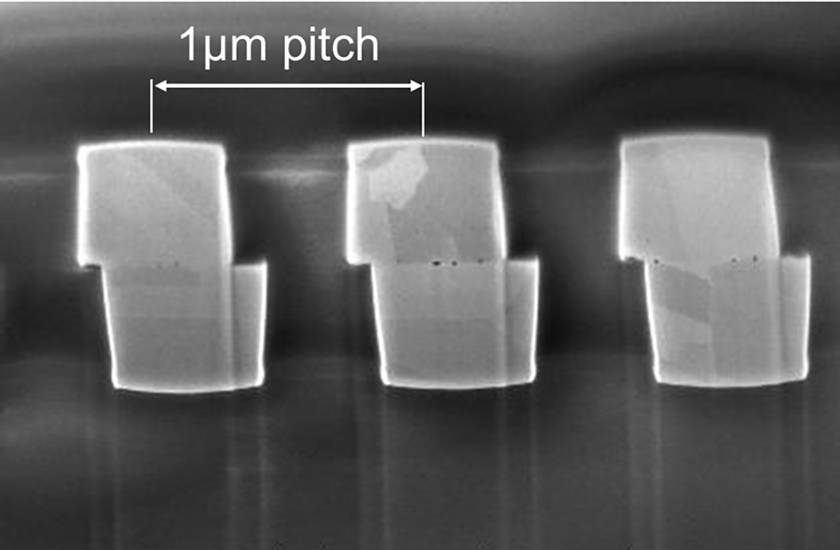
Focused Ion Beam Scanning Electron Microscope (FIB-SEM) cross-section of 1 micron pitch copper pads on a pair of 300-mm wafers. Photo courtesy of Leti.
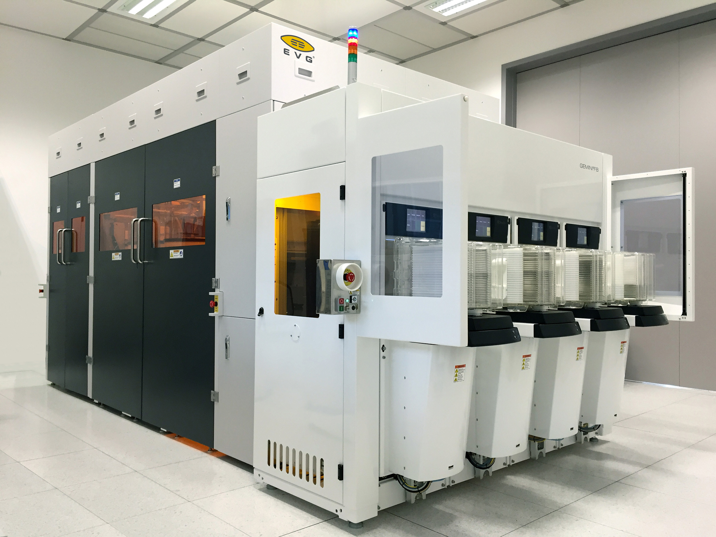
GEMINI®FB XT automated production fusion bonding system.
ST. FLORIAN, Austria and GRENOBLE, France, November 13, 2017 — EV Group (EVG), a leading supplier of wafer bonding and lithography equipment for the MEMS, nanotechnology and semiconductor markets, and Leti, an institute of CEA Tech, today announced the world's first successful 300-mm wafer-to-wafer direct hybrid bonding with pitch dimension connections as small as 1µm (micron). This breakthrough also achieved copper pads as small as 500nm.
The copper/oxide hybrid bonding process, a key enabler for 3D high-density IC applications, was demonstrated in Leti's cleanrooms using EVG's fully automated GEMINI®FB XT fusion wafer bonding system. This result was obtained in the framework of the program IRT Nanoelec headed by Leti. EVG joined the institute's 3D Integration Consortium in February 2016.
Wafer Bonding an Enabling Process for 3D Device Stacking
Vertical stacking of semiconductor devices has become an increasingly viable approach to enabling continuous improvements in device density and performance. Wafer-to-wafer bonding is an essential process step to enable 3D stacked devices. However, tight alignment and overlay accuracy between the wafers is required to achieve good electrical contact between the interconnected device on the bonded wafers, as well as to minimize the interconnect area at the bond interface so that more space can be made available on the wafer for producing devices. The constant reduction in pitches that are needed to support component roadmaps is fueling tighter wafer-to-wafer bonding specifications with each new product generation.
Demonstration Results
In the Leti demonstration, the top and bottom 300-mm wafers were directly bonded in the GEMINI FB XT automated production fusion bonding system, which incorporates EVG's proprietary SmartView®NT face-to-face aligner and an alignment verification module to enable in-situ post-bond IR alignment measurement. The system achieved overlay alignment accuracy to within 195nm (3-sigma) overall, with mean alignment results well centered below 15nm. Post-bake acoustic microscopy scans of the full 300-mm bonded wafer stack as well as specific dies confirmed a defect-free bonding interface for pitches ranging from 1µm to 4µm with optimum copper density.
"To our knowledge, this is the first reported demonstration of sub-1.5µm pitch copper hybrid bonding feasibility," said Frank Fournel, head of bonding process engineering at Leti. "This latest demonstration represents a real breakthrough and important step forward in enabling the achievement and eventual commercialization of high-density 3D chip stacking."
This demonstration is summarized in a paper co-authored by Leti, titled "1 µm Pitch Direct Hybrid Bonding with <300nm Wafer-to-wafer Overlay Accuracy," which was presented at the 2017 IEEE S3S Conference.
"3D integration holds the promise for increased device density and bandwidth as well as lower power consumption for a variety of applications, from next-generation CMOS image sensors and MEMS to high-performance computing," stated Markus Wimplinger, corporate technology development and IP director at EV Group. "As a leader in 3D integration research and development, Leti has been at the forefront in moving this critical technology toward industry adoption and commercialization. EVG shares that vision, and we are pleased to have played a role in supporting Leti's latest achievement in 3D integration."
Leveraging EVG's high-throughput XT Frame platform and an equipment front-end module (EFEM), the GEMINI FB XT automated production fusion bonding system is optimized for ultra-high throughput and productivity. The SmartView NT aligner integrated into the system provides industry-leading wafer-to-wafer overlay alignment accuracy (sub-200nm, 3-sigma). In addition, the GEMINI FB XT can accommodate up to six pre- and post-processing modules for surface preparation, conditioning and metrology steps such as wafer cleaning, plasma activation alignment verification, debonding (allowing pre-bonded wafers to be separated automatically and re-processed if necessary) and thermo-compression bonding.
EVG will showcase the GEMINI FB XT at the SEMICON Europa exhibition being held November 14-17 at the Messe München in Munich, Germany. Attendees interested in learning more about the product, as well as EVG's full suite of wafer bonding and lithography solutions, are invited to visit the company's booth
#B1-1424.
More information about EVG's GEMINI FB XT automated production fusion bonding system can be found here.
About Leti (France)
Leti, a technology research institute at CEA Tech, is a global leader in miniaturization technologies enabling smart, energy-efficient and secure solutions for industry. Founded in 1967, Leti pioneers micro-& nanotechnologies, tailoring differentiating applicative solutions for global companies, SMEs and startups. Leti tackles critical challenges in healthcare, energy and digital migration. From sensors to data processing and computing solutions, Leti's multidisciplinary teams deliver solid expertise, leveraging world-class pre-industrialization facilities. With a staff of more than 1,900, a portfolio of 2,700 patents, 91,500 sq. ft. of cleanroom space and a clear IP policy, the institute is based in Grenoble, France, and has offices in Silicon Valley and Tokyo. Leti has launched 60 startups and is a member of the Carnot Institutes network. This year, the institute celebrates its 50th anniversary.
Follow us on www.leti-cea.com and @CEA_Leti.
CEA Tech is the technology research branch of the French Alternative Energies and Atomic Energy Commission (CEA), a key player in innovative R&D, defence & security, nuclear energy, technological research for industry and fundamental science, identified by Thomson Reuters as the second most innovative research organization in the world. CEA Tech leverages a unique innovation-driven culture and unrivalled expertise to develop and disseminate new technologies for industry, helping to create high-end products and provide a competitive edge.
About EV Group (EVG)
EV Group (EVG) is a leading supplier of equipment and process solutions for the manufacture of semiconductors, microelectromechanical systems (MEMS), compound semiconductors, power devices and nanotechnology devices. Key products include wafer bonding, thin-wafer processing, lithography/nanoimprint lithography (NIL) and metrology equipment, as well as photoresist coaters, cleaners and inspection systems. Founded in 1980, EV Group services and supports an elaborate network of global customers and partners all over the world. More information about EVG is available at www.evgroup.com.
About Nanoelec Research Technological Institute (IRT)
Nanoelec Research Technological Institute (IRT), headed by CEA-Leti conducts research and development in the field of information and communication technologies (ICT) and, specifically, micro- and nanoelectronics. Based in Grenoble, France, IRT Nanoelec leverages the area's proven innovation ecosystem to create the technologies that will power the nanoelectronics of tomorrow, drive new product development and inspire new applications - like the Internet of Things - for existing technologies. The R&D conducted at IRT Nanoelec provides early insight into how emerging technologies such as 3D integration and silicon photonics will affect integrated circuits. Visit www.irtnanoelec.fr.
IRT Nanoelec benefits from French State aid under the "Programme Investissements d'Avenir" bearing reference ANR-10-AIRT-05.
Leti Press Contact:
Agency
Tel: +33 6 74 93 23 47
E-mail: sldampoux@mahoneylyle.comv
EV Group Contacts:
Clemens Schütte
Director, Marketing and Communications
EV Group
Tel: +43 7712 5311 0
E-mail: Marketing@EVGroup.com
David Moreno
Principal
Open Sky Communications
Tel: +1.415.519.3915
E-mail: dmoreno@openskypr.com
IRT Nanoelec Contact:
Didier Louis
Tel: +33 438783653
E-mail: didier.louis@cea.fr
Download PDF