DI Erich Thallner Strasse 1
4782 St. Florian am Inn
Austria
EV Group Unveils Next-Generation Fusion Wafer Bonder for “More Moore” Scaling and Front-End Processing
New BONDSCALE™ system provides a significant boost in wafer bond productivity; addresses logic transistor scaling and 3D integration challenges outlined in IRDS Roadmap
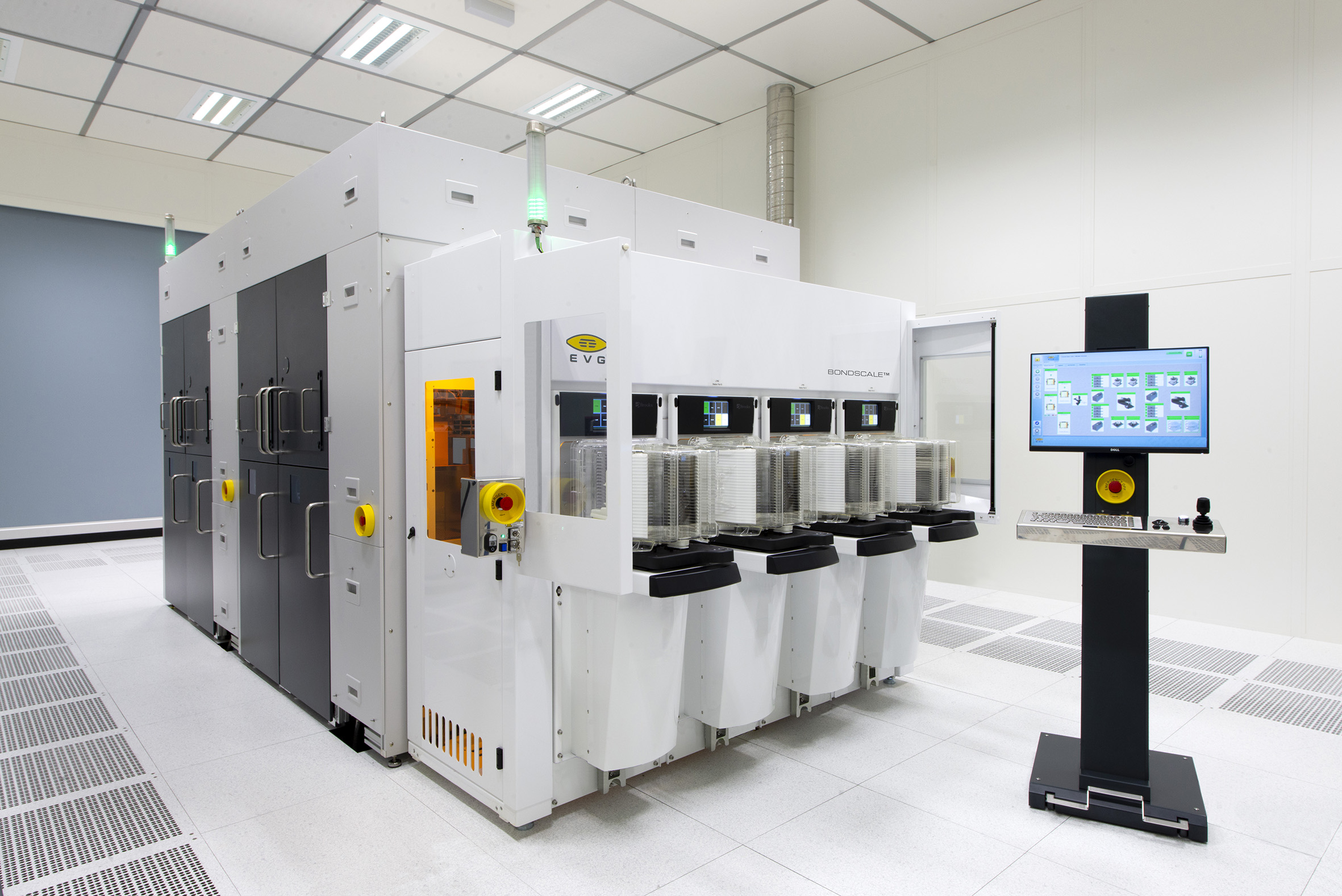
EVG BONDSCALE™ Automated Production Fusion Bonding System
ST. FLORIAN, Austria, December 3, 2018 — EV Group (EVG), a leading supplier of wafer bonding and lithography equipment for the MEMS, nanotechnology and semiconductor markets, today introduced the all new BONDSCALE™ automated production fusion bonding system. BONDSCALE is designed to fulfill a wide range of fusion/molecular wafer bonding applications, including engineered substrate manufacturing and 3D integration approaches that use layer-transfer processing, such as monolithic 3D (M3D). With BONDSCALE, EVG is bringing wafer bonding to front-end semiconductor processing and helping to address long-term challenges for “More Moore” logic device scaling identified in the International Roadmap for Devices and Systems (IRDS). Incorporating an enhanced edge alignment technology, BONDSCALE provides a significant boost in wafer bond productivity and lower cost of ownership (CoO) compared to existing fusion bonding platforms. It is already being shipped to customers.
BONDSCALE is being sold alongside EVG’s industry benchmark GEMINI® FB XT automated fusion bonding system, with each platform targeting different applications. While BONDSCALE will primarily focus on engineered substrate bonding and layer-transfer processing, the GEMINI FB XT will support applications requiring higher alignment accuracies, such as memory stacking, 3D systems on chip (SoC), backside illuminated CMOS image sensor stacking, and die partitioning.
Direct wafer bonding key to driving semiconductor performance scaling
According to the IRDS Roadmap, parasitic scaling will become a dominant driver of logic device performance in the coming years, requiring new transistor architectures and materials. The IRDS Roadmap also notes that new 3D integration approaches such as M3D will be necessary to support the long-term transition from 2D to 3D VLSI, including backside power distribution, N&P stacking, logic-on-memory, clustered functional stacks and beyond-CMOS adoption. Layer transfer processes and engineered substrates are enabling technologies for logic scaling by helping to deliver significant improvements in device performance, functionality and power consumption. Direct wafer bonding with plasma activation is a proven solution for enabling heterogeneous integration of different materials, high-quality engineered substrates as well as thin-silicon layer transfer applications.
“As a pioneer and market leader in wafer bonding, EVG has been at the forefront in helping customers bring new semiconductor technologies from early R&D to full-scale manufacturing,” stated Paul Lindner, executive technology director at EV Group. “Nearly 25 years ago, EVG introduced the industry’s first silicon-on-insulator (SOI) wafer bonder to support the production of high-frequency and radiation-hard devices for niche applications. Since then, we have continuously enhanced the performance and CoO of our direct bonding platforms to help our customers bring the benefits of engineered substrates to a wider range of applications. Our new BONDSCALE solution takes this to the next level, boosting productivity to fulfill the growing need for engineered substrates and layer-transfer processing to enable continued performance, power and area scaling of next-generation logic and memory devices in the ‘More Moore’ era.”
BONDSCALE is a high-volume production system for fusion/direct wafer bonding needed for front-end-of-line applications. Featuring EVG’s LowTemp™ plasma activation technology, the BONDSCALE system combines all essential steps for fusion bonding—including cleaning, plasma activation, alignment, pre-bonding and IR inspection—in a single platform that is suitable for a wide range of fusion/molecular wafer bonding applications. Capable of processing both 200-mm and 300-mm wafers, the system ensures a void-free, high-throughput, and high-yield production process.
BONDSCALE incorporates next-generation fusion/direct bonding modules, a new wafer handling system and optical edge alignment to provide significantly higher throughput and productivity to support the needs of its customers to ramp up engineered substrate wafer production and M3D integration.
More information about the BONDSCALE automated fusion production bonding system for engineered substrate and front-end wafer bonding can be found here.
About EV Group (EVG)
EV Group (EVG) is a leading supplier of equipment and process solutions for the manufacture of semiconductors, microelectromechanical systems (MEMS), compound semiconductors, power devices and nanotechnology devices. Key products include wafer bonding, thin-wafer processing, lithography/nanoimprint lithography (NIL) and metrology equipment, as well as photoresist coaters, cleaners and inspection systems. Founded in 1980, EV Group services and supports an elaborate network of global customers and partners all over the world. More information about EVG is available at www.EVGroup.com.
Contacts:
Clemens Schütte
Director, Marketing and Communications
EV Group
Tel: +43 7712 5311 0
E-mail: Marketing@EVGroup.com
David Moreno
Principal
Open Sky Communications
Tel: +1.415.519.3915
E-mail: dmoreno@openskypr.com