DI Erich Thallner Strasse 1
4782 St. Florian am Inn
Austria
EV Group Receives Multiple Lithography and Metrology System Orders for Wafer-level Optics Manufacturing
Demand for manufacturing solutions driven by consumer electronics, mobile and other applications requiring advanced 3D / optical sensors
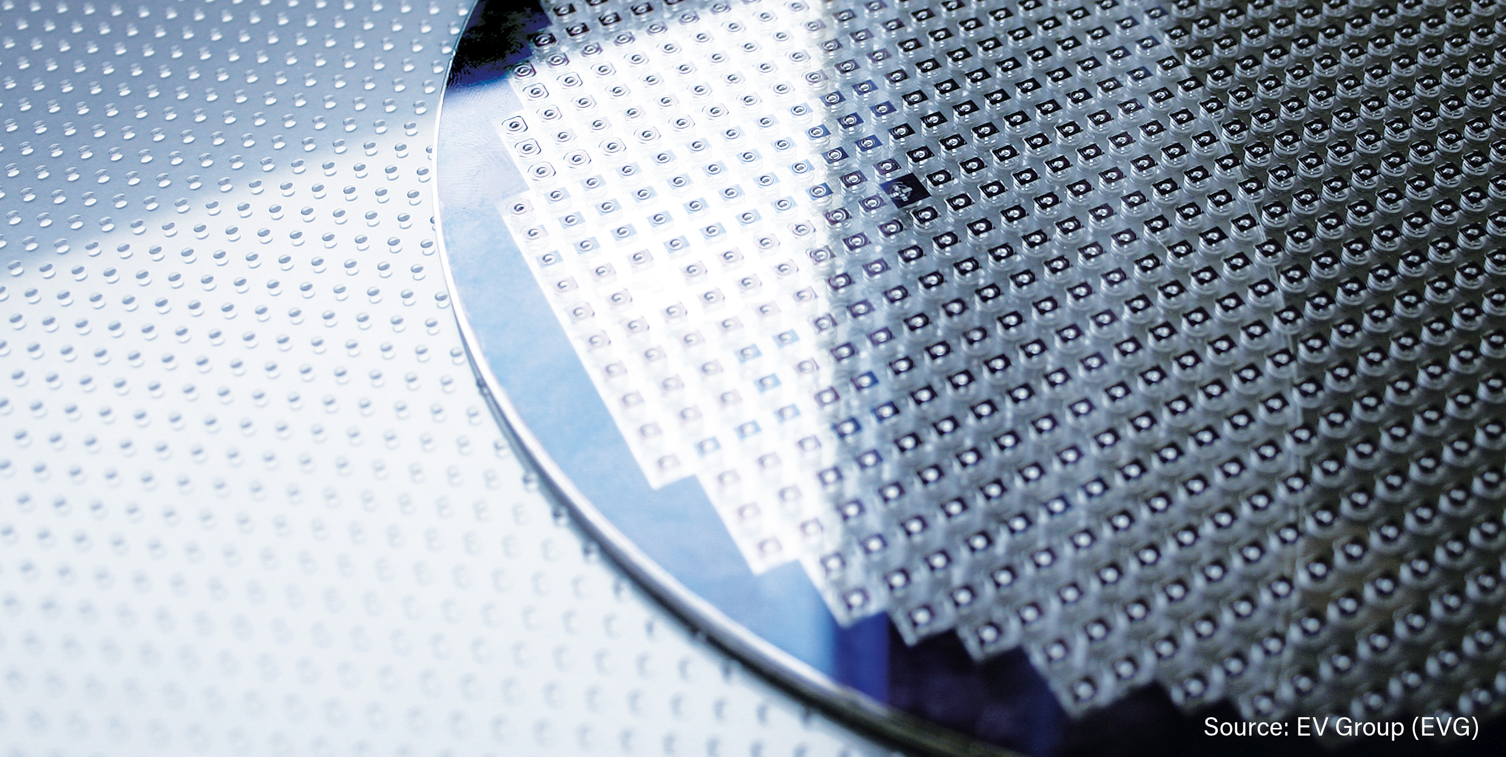
Lens wafer fabricated with EVG's soft UV imprint lithography technology and a bonded micro optics stack consisting of lens wafers and spacer wafers
ST. FLORIAN, Austria, September 11, 2017 – EV Group (EVG), a leading supplier of wafer bonding and lithography equipment for the MEMS, nanotechnology and semiconductor markets, today announced it has received multiple orders for its comprehensive portfolio of manufacturing equipment and services designed to address the burgeoning demand for wafer-level optics (WLO) and 3D sensing. The market-leading portfolio comprises the EVG®770 automated UV-nanoimprint lithography (UV-NIL) stepper for step-and-repeat master stamp fabrication, the IQ Aligner® UV imprinting system for wafer-level lens molding and stacking, and the EVG®40 NT automated measurement system for alignment verification. EVG's WLO solutions are supported by the company's NILPhotonics® Competence Center, which leverages field-proven process and equipment know-how to support emerging photonic applications and significantly shorten time to market through fast process implementation and optimization, as well as through customized equipment design.
Using state-of-the-art imprint lithography and bond-alignment technologies to fabricate microlenses, diffractive optical elements and other optical components at the wafer-level provides numerous benefits. These include lowering cost of ownership through highly parallel fabrication processes, as well as enabling smaller form factors of the final devices through stacking. EVG is both a pioneer and market leader in nanoimprint lithography and micromolding with the largest installed base of tools worldwide.
"We are seeing a steep increase in the demand for equipment enabling wafer-level optics," confirmed Dr. Thomas Glinsner, corporate technology director for EV Group. "Since the beginning of this year alone, we have shipped multiple systems for lens molding and stacking as well as metrology to major WLO manufacturers for high-volume production. Such orders are further strengthening EVG's position as the market leader in this area, while creating a wealth of new opportunities in emerging applications."
Industry-leading device makers have recently announced plans to broaden their business targets in the sensing space to help address customers' increasingly aggressive time-to-market windows. According to market research and strategy consulting firm Yole Développement, more than a dozen types of sensors are being designed into next-generation smartphones. These include 3D sensing cameras, fingerprint sensors, iris scanners, laser diode emitters, laser rangers and biosensors. Overall, the optical hub is expected to grow from $10.6 billion in 2016 to $18 billion by 2021, showing a compound annual growth rate of more than 11 percent*.
Demand for EVG's WLO manufacturing solutions is driven in part by the need for novel optical sensing solutions and devices for mobile consumer electronics products. Key examples include 3D sensing (essential for more authentic virtual and augmented reality (VR/AR) user experiences), biometric sensing (increasingly critical for security applications), environmental sensing, infrared (IR) sensing and camera arrays. Other applications include additional optical sensors in smartphones for advanced depth sensing to improve camera autofocus performance, and micro displays.
"There is undoubtedly a highly sustainable trend emerging in wafer-level optics and 3D sensing," stated Markus Wimplinger, EV Group's corporate technology development and IP director. "We foresee even broader adoption of this technology in the near future due to the large number of ongoing customer projects supported by our NILPhotonics Competence Center located at our corporate headquarters."
EVG's WLO equipment portfolio includes:
- EVG770 automated UV-NIL stepper for master stamp fabrication. Master stamps are wafer-size templates fully populated with microlens molds each replicated from one single lens template in a step-and-repeat approach. Starting out from a single lens master made out of metal or glass, EVG offers a process flow that covers all essential process steps for the fabrication of master stamps, featuring unmatched lens position accuracy and high lens shape repeatability required for the fabrication of high-end wafer-level camera modules.
- IQ Aligner automated UV-NIL system for UV microlens molding. Soft UV imprint lithography is a highly parallel technique for the fabrication of polymeric microlenses, the key elements of WLO systems. Starting out from soft working stamps replicated from wafer-size master stamps, EVG offers hybrid and monolithic microlens molding processes that can be easily adapted to various material combinations for working stamp and microlens materials. In addition, EV Group offers a qualified microlens molding process, including all relevant material know-how.
- EVG40 NT automated measurement system. Supporting vertical as well as lateral measurements with very-high resolution and accuracy, metrology is crucial to verify compliance to tight process specifications and instantly optimize integrated process parameters. In WLO manufacturing, EVG's metrology solutions can be used for critical dimension (CD) measurement and lens stack alignment verification, as well as many other applications.
EVG will showcase its WLO portfolio at the SEMICON Taiwan exhibition being held September 13-15 at the Taipei Nangang Exhibition Center. Attendees interested in learning more about the products, as well as EVG's full suite of lithography and wafer bonding solutions, are invited to visit the company's booth #212.
* Note to Editors: The source for this market data is the "Sensors for Cellphones and Tablets 2016" report, released by Yole Développement in June 2016. More information on the report is available at: www.i-micronews.com/category-listing/product/sensors-for-cellphones-and-tablets-2016.html.
About EV Group (EVG)
EV Group (EVG) is a leading supplier of equipment and process solutions for the manufacture of semiconductors, microelectromechanical systems (MEMS), compound semiconductors, power devices and nanotechnology devices. Key products include wafer bonding, thin-wafer processing, lithography/nanoimprint lithography (NIL) and metrology equipment, as well as photoresist coaters, cleaners and inspection systems. Founded in 1980, EV Group services and supports an elaborate network of global customers and partners all over the world. More information about EVG is available at www.EVGroup.com.
Contacts:
Clemens Schütte
Director, Marketing and Communications
EV Group
Tel: +43 7712 5311 0
E-mail: Marketing@EVGroup.com
David Moreno
Principal
Open Sky Communications
Tel: +1.415.519.3915
E-mail: dmoreno@openskypr.com