DI Erich Thallner Strasse 1
4782 St. Florian am Inn
Austria
EV Group Expands High-Vacuum Wafer Bonding Capabilities of EVG ComBond Platform for High-Volume MEMS Manufacturing
New wafer alignment and bake modules provide critical capabilities to support wafer bonding for a broad range of new and emerging MEMS manufacturing applications
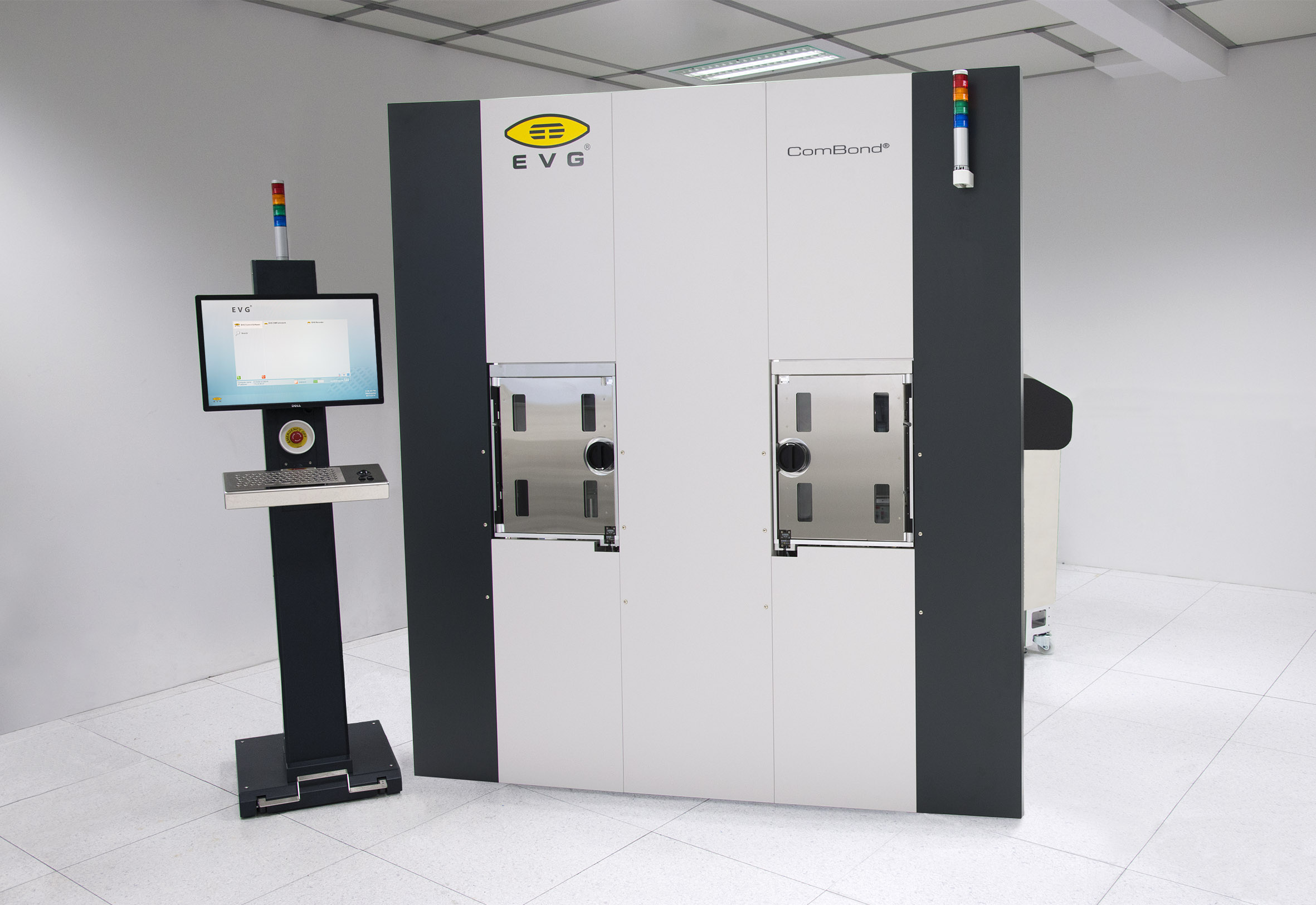
EVG ComBond® Automated High-Vacuum Wafer Bonding System
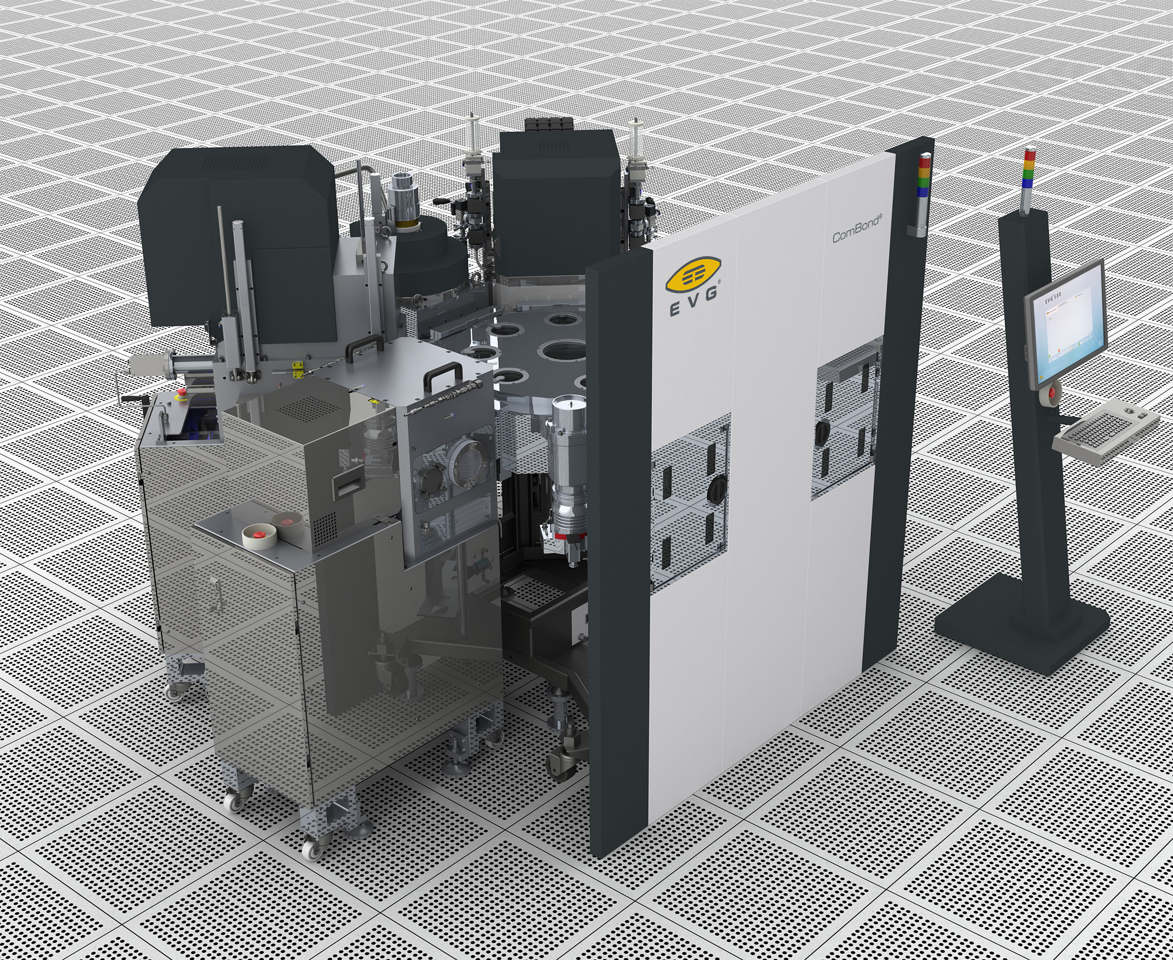
EVG ComBond® Platform
ST. FLORIAN, Austria, July 6, 2016 — EV Group (EVG), a leading supplier of wafer bonding and lithography equipment for the MEMS, nanotechnology and semiconductor markets, today introduced new capabilities on the EVG ComBond® automated high-vacuum wafer bonding platform specifically designed to support high-volume manufacturing (HVM) of advanced MEMS devices. These capabilities include a new vacuum bond alignment module that provides sub-micron face-to-face alignment accuracy essential for wafer-level MEMS packaging, and a new bake module that performs critical process steps to achieve outstanding bond quality and performance of encapsulated MEMS devices.
The addition of these two new modules-coupled with existing capabilities on the highly configurable EVG ComBond platform such as room-temperature covalent bonding of engineered substrates-enables customers to meet the wafer bonding requirements for both current and emerging types of MEMS devices. Examples include gyroscopes, microbolometers, and advanced sensors for autonomous cars, virtual reality headsets and other applications.
"When EV Group introduced the EVG ComBond platform, we set a new standard in high-vacuum wafer bonding by building the product around a modular, highly customizable cluster design concept. This has enabled us to continually expand the capabilities of the platform over time, with applications ranging from advanced engineered substrates, power devices and solar cells to high-performance logic and 'Beyond CMOS' devices," stated Paul Lindner, executive technology director, EV Group. "With the addition of new vacuum alignment and bake modules, those wafer bonding capabilities have been expanded yet again to address the volume manufacturing needs for high-end MEMS devices."
Challenges of Scaling MEMS Wafer Bonding into Production
Many MEMS devices have extremely small moving parts, which must be protected from the external environment. Wafer-level capping can seal a wafer's worth of MEMS devices in one operation, and these capped devices can then be packaged into much simpler and lower-cost packages. Metal-based aligned wafer bonding is the preferred approach to MEMS wafer bonding, but is challenging to implement due to the high process temperatures involved as well as the presence of oxides that form on the bonding metal layers. As MEMS die and feature sizes decrease, achieving tighter wafer alignment accuracy also becomes increasingly important.
At the same time, vacuum encapsulation is increasingly needed for certain MEMS devices in order to reduce power consumption caused by parasitic drag, reduce convection heat transfer, or prevent oxide corrosion. Maintaining the required vacuum level for the entire wafer bonding process has been a key challenge for ramping these devices into high-volume production.
The EVG ComBond platform provides a complete end-to-end high-vacuum environment (10-8 mbar range) throughout all wafer handling, pre-bonding and bonding processes. This modular configuration significantly improves serviceability, as modules can be swapped out without breaking the vacuum level within the cluster or modules and interrupting tool operation.
New MEMS Wafer Bonding Capabilities
New to the EVG ComBond platform is the vacuum alignment module (VAM) with wafer clamping, which enables sub-micron face-to-face alignment accuracy based on EVG's proprietary SmartView® alignment process, as well as backside and IR alignment, in a high-vacuum environment. Also new is the programmable dehydration bake and getter activation module, which accelerates the removal of sticking gas molecules prior to bonding the substrates-resulting in improved bond quality as well as reduced gas pressure in device cavities.
In addition, the EVG ComBond platform features an optional ComBond Activation Module (CAM), which enables covalent and oxide-free wafer bonding processes at room temperature or low temperatures. Integrated into the ComBond platform, the CAM allows low-temperature bonding of metals, such as aluminum, that re-oxidize quickly in ambient environments-enabling customers to reduce production costs and achieve higher wafer-bonding throughputs.
The EVG ComBond platform with the new alignment and programmable dehydration bake and getter activation modules is currently available and can be demonstrated at EVG's headquarters.
Media, analysts and potential customers interested in learning more about EVG's suite of wafer bonding solutions, including the EVG ComBond platform, are invited to visit the company's booth #1017 in the South Hall of the Moscone Convention Center in San Francisco, Calif., at the SEMICON West show on July 12-14.
About EV Group (EVG)
EV Group (EVG) is a leading supplier of equipment and process solutions for the manufacture of semiconductors, microelectromechanical systems (MEMS), compound semiconductors, power devices and nanotechnology devices. Key products include wafer bonding, thin-wafer processing, lithography/nanoimprint lithography (NIL) and metrology equipment, as well as photoresist coaters, cleaners and inspection systems. Founded in 1980, EV Group services and supports an elaborate network of global customers and partners all over the world. More information about EVG is available at www.EVGroup.com.
Contacts:
Clemens Schütte
Director, Marketing and Communications
EV Group
Tel: +43 7712 5311 0
E-mail: Marketing@EVGroup.com
David Moreno
Principal
Open Sky Communications
Tel: +1.415.519.3915
E-mail: dmoreno@openskypr.com