DI Erich Thallner Strasse 1
4782 St. Florian am Inn
Austria
EV Group Wins Global Technology Award for MLE™ Maskless Exposure Technology at productronica and SEMICON Europa
EVG’s breakthrough MLE™ technology provides unsurpassed flexibility, scalability and cost-of-ownership benefits compared to existing high-volume-manufacturing lithography methods
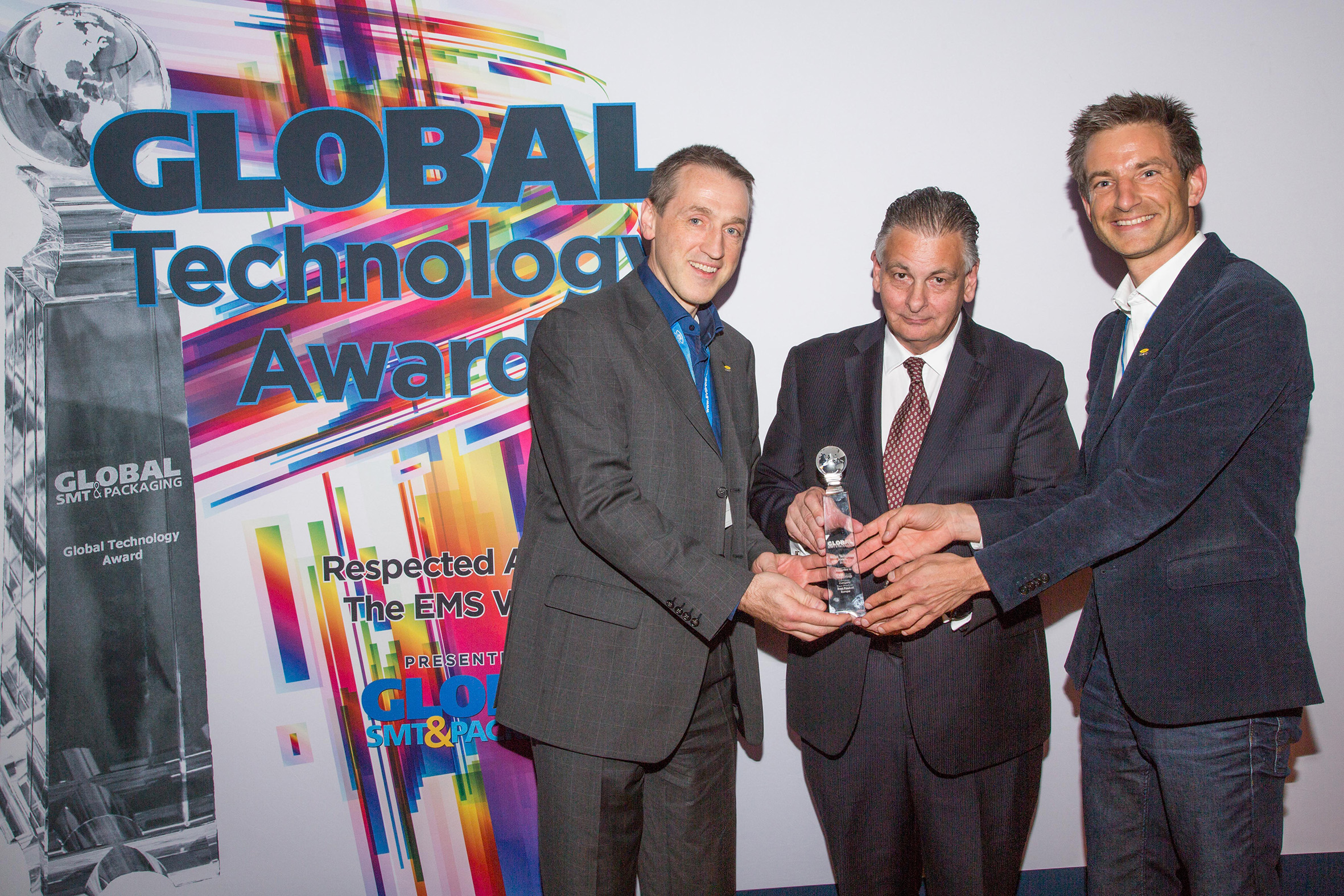
Trevor Galbraith, Editor-in-Chief of Global SMT & Packaging magazine, presents the GLOBAL Technology Award to EV Group
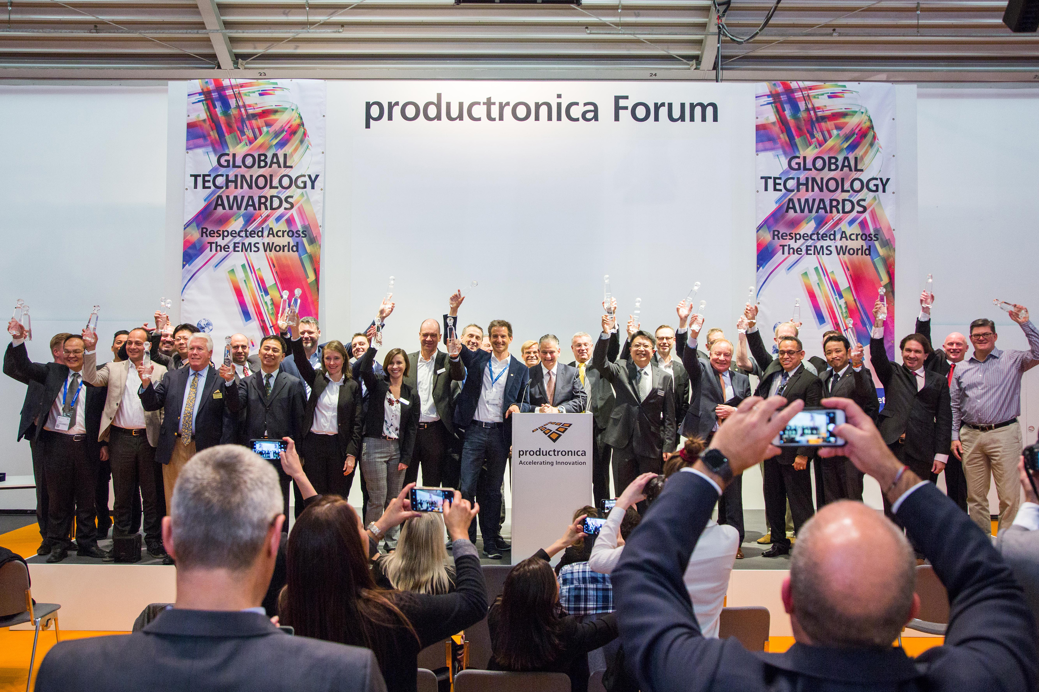
GLOBAL Technology Awards ceremony held in conjunction with the productronica and SEMICON Europa 2019 tradeshows in Munich, Germany
ST. FLORIAN, Austria, November 12, 2019—EV Group (EVG), a leading supplier of wafer bonding and lithography equipment for the MEMS, nanotechnology and semiconductor markets, has been recognized by Global SMT Packaging with a GLOBAL Technology Award for Best Product - Europe for the company’s groundbreaking MLE™ maskless exposure technology. EVG was honored among a select group of companies at an awards ceremony held in conjunction with the productronica and SEMICON Europa 2019 tradeshows in Munich, Germany, which featured the very latest innovative products and technologies introduced by suppliers of electronics manufacturing equipment and materials over the past 12 months.
EVG’s MLE technology is a revolutionary next-generation lithography technology developed to address future back-end lithography needs for advanced packaging, MEMS, biomedical and high-density printed circuit board (HD PCB) applications. The world’s first highly scalable maskless lithography technology for high-volume manufacturing, MLE delivers unsurpassed flexibility to enable extremely short development cycles for new devices.
“We are honored to receive this prestigious award for our MLE technology, which is a revolutionary breakthrough in back-end lithography. Heterogeneous integration is pushing up the requirements for back-end lithography, which in turn is driving the need for new lithography approaches that no longer have to compromise on performance or cost. Our MLE technology is designed to meet the future challenges of back-end lithography and fulfill all requirements for adaptive patterning for advanced packaging and high-density interconnect PCBs. It is gratifying to see the merits of this breakthrough technology recognized by the award judges,” stated Dr. Bernd Thallner, corporate R&D project manager at EV Group.
MLE enables high-resolution (<2 microns L/S), stitch-free maskless exposure of the entire substrate surface with high throughput and low cost of ownership. The system scales according to user needs by adding or removing UV exposure heads – for facilitating rapid transition from R&D to high-volume manufacturing (HVM) mode, for throughput optimization, or for adaptation to different substrate sizes and materials – and is ideal for processing a range of substrates from small silicon or compound semiconductor wafers up to panel sizes. MLE achieves the same patterning performance regardless of photoresist thanks to a flexible and scalable high-power UV laser source, which provides multiple wavelength exposure options.
For more information about EVG’s MLE maskless exposure technology, please visit https://www.evgroup.com/technologies/mle-maskless-lithography/.
About EV Group (EVG)
EV Group (EVG) is a leading supplier of equipment and process solutions for the manufacture of semiconductors, microelectromechanical systems (MEMS), compound semiconductors, power devices and nanotechnology devices. Key products include wafer bonding, thin-wafer processing, lithography/nanoimprint lithography (NIL) and metrology equipment, as well as photoresist coaters, cleaners and inspection systems. Founded in 1980, EV Group services and supports an elaborate network of global customers and partners all over the world. More information about EVG is available at www.EVGroup.com.
Contacts:
Clemens Schütte
Director, Marketing and Communications
EV Group
Tel: +43 7712 5311 0
E-mail: Marketing@EVGroup.com
David Moreno
Principal
Open Sky Communications
Tel: +1.415.519.3915
E-mail: dmoreno@openskypr.com