DI Erich Thallner Strasse 1
4782 St. Florian am Inn
Austria
EV Group Extends Volume Manufacturing Expertise to Biotechnology and Medical Device Applications
EVG leverages more than 15 years of experience in biotech R&D and industry-proven substrate bonding and lithography solutions and expertise to support next-generation biotechnology device manufacturing
EV Group NIL solutions enable parallel processing of devices on large area substrates
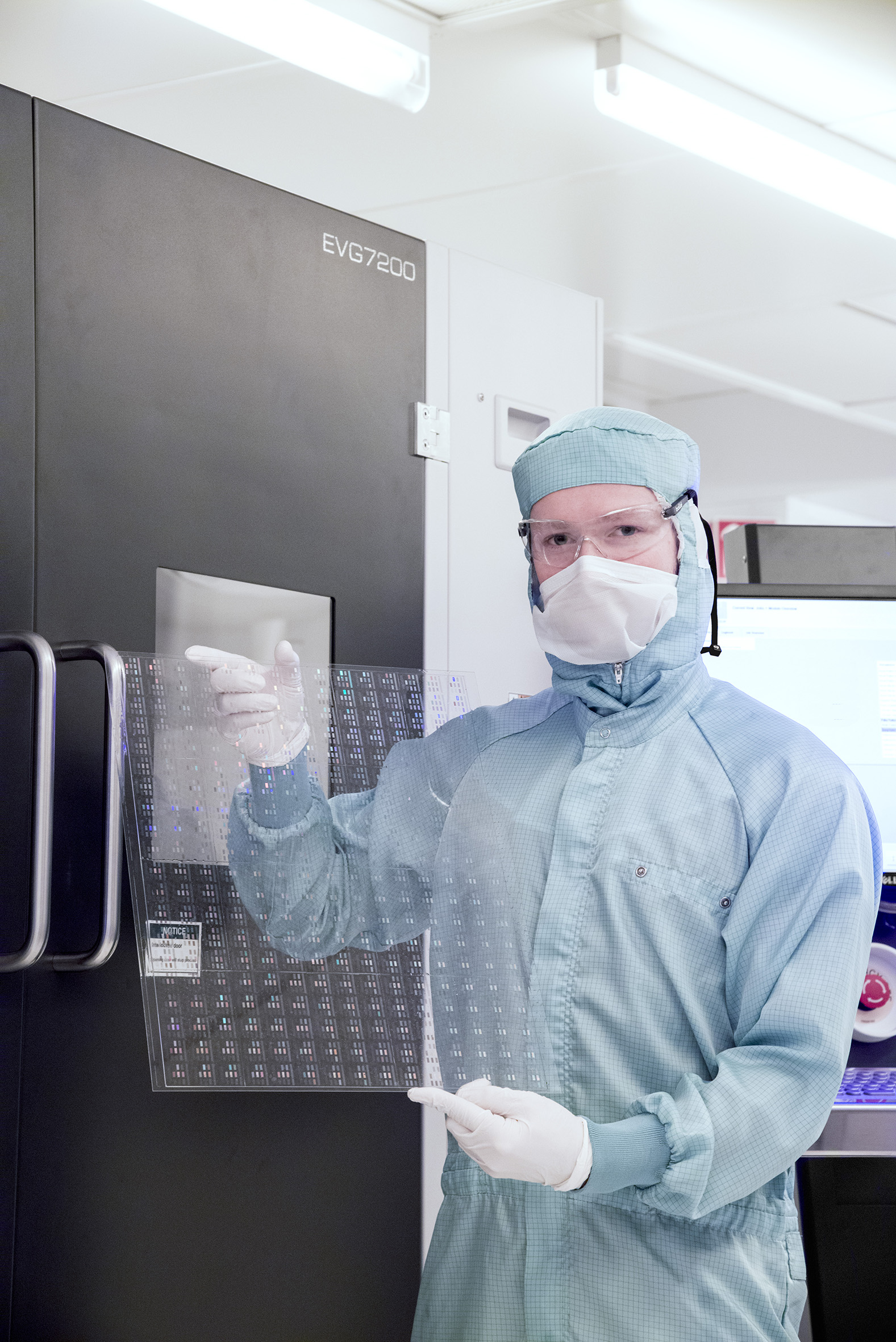
ST. FLORIAN, Austria, September 26, 2016 — EV Group (EVG), a leading supplier of wafer bonding and lithography equipment for the MEMS, nanotechnology and semiconductor markets, today announced that it is increasing its focus on bringing its high-volume manufacturing process solutions and services to the biotechnology and medical device market. EVG products supporting this market include the company's substrate bonding, hot-embossing, micro contact printing and UV-based nanoimprint lithography (NIL) systems. In addition, EVG will offer its world-class applications support, rapid prototyping and pilot-line production services. Customers in the biotechnology and medical markets can now leverage these patterning and sealing solutions-which have been production-proven in other industrial markets such as semiconductors, MEMS and photonics-for volume production of next-generation biotechnology devices featuring micrometer or nanometer-scale patterns and structures on larger-format substrates.
Over the past several decades, miniaturization of biotechnology devices has significantly improved clinical diagnostics, pharmaceutical research and analytical chemistry. Modern biotechnology devices-such as biomedical MEMS (bioMEMS) for diagnostics, cell analysis and drug discovery-are often chip-based and rely on close interaction of biological substances at the micro- and nanoscale. According to the market research and strategy consulting firm Yole Développement, an increasing number of healthcare applications are using bioMEMS components, while the bioMEMS market is expected to triple from US$2.7 billion in 2015 to US$7.6 billion in 2021. Microfluidic devices will represent the majority (86 percent) of the total bioMEMS market in 2021, driven by applications such as Point-of-Need testing, clinical and veterinary diagnostics, pharmaceutical and life science research, and drug delivery*.
Precise and cost-effective micro-structuring technologies are essential to successfully commercialize these products in a rapidly growing market that has stringent requirements and high regulatory hurdles. Traditional process approaches such as injection molding are often unable to produce the extremely small structures and surface patterns with the precision, quality and repeatability increasingly required for these demanding applications, or they require extensive effort in process development. At the same time, solutions are needed to scale up from discrete production of devices to batch processing of multiple devices on a single substrate in order to achieve the economies of scale required to commercialize these products.
NIL has evolved from a niche technology to a powerful high-volume manufacturing method that is able to produce a multitude of structures of different sizes and shapes on a large scale-such as highly complex microfluidic channels and surface patterns-by imprinting either into a biocompatible resist or directly into the bulk material. In addition to structuring technologies, sealing and encapsulation is a central process for establishing confined microfluidic channels. Thus, bonding of different device layers, capping layers or interconnection layers is a key process that can be implemented together with NIL in a cost-effective large-area batch process. As the pioneer as well as market and technology leader in NIL and wafer bonding, EVG is leading the charge in supporting the infrastructure and growth of the biotechnology market by leveraging its products for use in biotechnology applications.
EVG's NIL solutions can produce a wide range of small structures (from hundreds of micrometers down to 20 nm) on a variety of substrate materials used in biotechnology applications, including glass, silicon and a variety of polymers (e.g., COC, COP, PMMA and PS). Each EVG NIL solution is uniquely suited for different production applications. For example, hot-embossing allows precise imprinting of larger structures as well as combinations of micro- and nanostructures, and is superior when replicating high-aspect ratio features or when using very-thin substrates. UV-NIL provides very-high precision, pattern fidelity and throughput in the nanometer-range. Micro contact printing, which is another NIL option, can transfer materials such as biomolecules onto a substrate in a distinct pattern.
With its established wafer-scale bonding equipment, EVG can also offer sealing and bonding processes that are well-aligned with NIL structuring technologies. A variety of different bonding options are available, ranging from advanced room-temperature bonding techniques to plasma activated bonding as well as high-quality hermetic sealing and vacuum encapsulation. Examples of typical solutions include EVG's thermal bonding equipment for glass and polymer substrates, which provides excellent results by enabling high-pressure and temperature uniformities over large areas. EVG also offers its room-temperature selective adhesive transfer technology, which eases incorporation of bio-molecules prior to the encapsulation of the device.
"EVG has a long history of providing products and solutions for biomedical R&D, having installed the first hot embossing system for emerging bioMEMS and microfluidic research applications more than 15 years ago," stated Dr. Thomas Uhrmann, director of business development at EV Group. "The knowledge that EVG has built up in this space coupled with our experience in bringing innovative technologies into volume production in other markets has positioned us well to provide proven high-volume manufacturing processes and services to the bio-medical industry to support the production of next-generation biotechnology devices."
In addition to equipment and process solutions, EVG also offers prototyping and pilot-line production services to customers out of its cleanroom facilities at its corporate headquarters in Austria as well as its subsidiaries in North America and Japan.
More information on EVG's suite of process solutions for the biotechnology and medical device market can be found here. In addition, EVG will showcase these solutions at the Lab-on-a-Chip Microfluidics & Microarrays World Congress being held September 26-28 at the Marriott Mission Valley Hotel in San Diego, Calif. Attendees interested in learning more about EVG's suite of biotechnology solutions are invited to visit the company's booth C48 throughout the show, as well as attend EVG's Technology Spotlight presentation during the session "From Technologies to Utility - Applications of Microfluidics/LOAC in Life Sciences and Beyond" on Wednesday, September 28 from 11:45 a.m. to 12:15 p.m. Pacific Time.
About EV Group (EVG)
EV Group (EVG) is a leading supplier of equipment and process solutions for the manufacture of semiconductors, microelectromechanical systems (MEMS), compound semiconductors, power devices and nanotechnology devices. Key products include wafer bonding, thin-wafer processing, lithography/nanoimprint lithography (NIL) and metrology equipment, as well as photoresist coaters, cleaners and inspection systems. Founded in 1980, EV Group services and supports an elaborate network of global customers and partners all over the world. More information about EVG is available at www.EVGroup.com.
Contacts:
Clemens Schütte
Director, Marketing and Communications
EV Group
Tel: +43 7712 5311 0
E-mail: Marketing@EVGroup.com
David Moreno
Principal
Open Sky Communications
Tel: +1.415.519.3915
E-mail: dmoreno@openskypr.com
* Note to Editors: The source for this market data is the "BioMEMS: Microsystems for Healthcare Applications 2016" report, released by Yole Développement in April 2016.