DI Erich Thallner Strasse 1
4782 St. Florian am Inn
Austria
EV Group Achieves Breakthrough in Hybrid Bonding Overlay Control for Chiplet Integration
New EVG®40 D2W overlay metrology system provides 100 percent overlay measurement on every die at up to 15X higher throughput versus industry benchmark
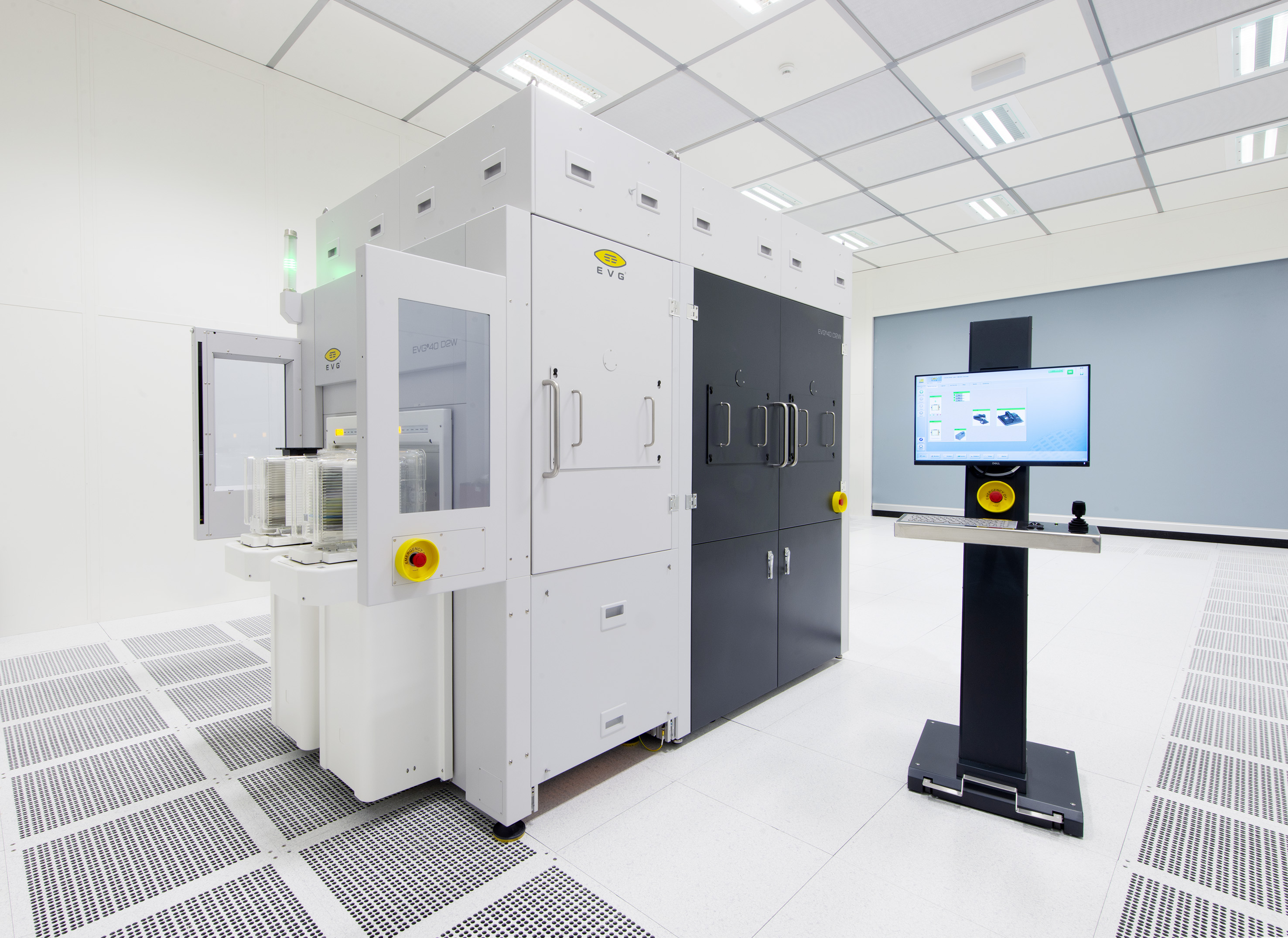
The EVG®40 D2W system is the first dedicated die-to-wafer overlay metrology platform to deliver 100 percent die overlay measurement on 300-mm wafers at high precision and speeds needed for production environments.
ST. FLORIAN, Austria, September 8, 2025—EV Group (EVG), a leading provider of innovative process solutions and expertise serving leading-edge and future semiconductor designs and chip integration schemes, today unveiled the EVG®40 D2W—the first dedicated die-to-wafer overlay metrology platform to deliver 100 percent die overlay measurement on 300-mm wafers at high precision and speeds needed for production environments. With up to 15X higher throughput than EVG’s industry benchmark EVG®40 NT2 system designed for hybrid wafer bonding metrology, the new EVG40 D2W enables chipmakers to verify die placement accuracy and take rapid corrective action, improving process control and yield in high-volume manufacturing (HVM).
The EVG40 D2W can be used for any D2W bonding application, including chiplet integration, high-bandwidth memory (HBM) stacks, and 3D system on chip (SoC) integration processes, which enable high-performance devices for artificial intelligence (AI), high-performance computing (HPC), data centers and other applications. Multiple EVG40 D2W systems have already been installed at customer sites and are being used in HVM production services.
EVG executives will be available to discuss the EVG40 D2W system, as well as industry developments in chiplet integration, hybrid bonding and other important updates at SEMICON Taiwan, taking place this week in Taipei, Taiwan, September 8-12.
D2W Bonding Enables High-Performance Devices
D2W bonding integrates diverse dies or chiplets of different sizes, materials, and functions into a single device or package. This is essential for creating devices and systems that meet the increased performance demands of applications like AI and autonomous driving, with lower power consumption. As interconnect pitches in 3D packaging become tighter with each new product generation, die bond alignment and overlay processes must also scale accordingly, not only with greater accuracy but also higher measurement coverage, to identify overlay errors that can lead to misaligned copper pads or bond interfaces and result in yield loss.
Legacy Overlay Metrology Methods Ill-Matched for D2W Bonding
Current D2W bond overlay metrology systems utilize “move-acquire-measure” techniques inherited from wafer-to-wafer (W2W) bond overlay metrology systems, which exceed the measurement precision while lacking the throughput necessary for D2W bond overlay metrology. To achieve faster run rates, these systems must reduce sampling sizes, resulting in sparse alignment information that can lead to inaccurate feedback for process correction. At the same time, integrated metrology solutions in pick and place D2W bonding systems are less flexible and do not have sufficient accuracy for leading-edge applications.
Dedicated D2W Overlay Metrology with EVG40 D2W
The EVG40 D2W has several hardware and software enhancements to achieve precise 100 percent overlay measurements across all dies on a 300-mm wafer without impacting throughput:
- Enhanced throughput via dual-layer measurement of alignment targets on both the die and the base wafer in a single pass
- High-speed precision from a new stage design, which ensures synchronization between image capture and stage movement
- Consistent accuracy thanks to a modified light source, which maintains proper levels of illumination for precise measurements
- High-quality image capture enabled by large focal offset, ensuring high signal-to-noise ratio when the focal plane of alignment targets differs between base and top chiplets
According to Paul Lindner, executive technology director at EV Group, “As a leader in hybrid bonding,
EV Group is steadfast in its commitment to developing new products and capabilities that push the performance envelope and solve our customers’ most complex integration problems. The die-to-wafer bonding process is particularly challenging since the integration of different types of chips, nodes and materials requires comprehensive metrology in production environments to better understand and improve the bonding process without sacrificing throughput. We are therefore pleased to introduce the EVG40 D2W, the newest addition to our portfolio of die-to-wafer bonding solutions. Designed from the ground up as a dedicated D2W metrology tool, the EVG40 D2W delivers the highest throughput of any system in its class. We look forward to working closely with our customers and partners to leverage this new D2W bonding solution to optimize their hybrid bonding processes for their latest products.”
EVG40 D2W Key Features and Benefits
- Measures up to 2800 overlay measurement points across the wafer in just four minutes, delivering 100 percent die positioning feedback without sacrificing throughput
- Measurement precision supports requirements for leading-edge D2W bonding applications
- Uses an advanced model to calculate placement, distortion, rotation and run-out variation for each die
- Feeds measurement results back to the fab’s host system for analysis, enabling optimization of D2W overlay and bonding process for future wafer runs
- Can be used alongside any third-party D2W bonding system to ensure the highest possible level of quality control
- Complements EVG’s suite of tools for D2W bonding, including the EVG320 D2W activation and cleaning system
See EVG at SEMICON Taiwan 2025
Attendees at SEMICON Taiwan interested in learning more about the EVG40 D2W and other innovative process solutions from EVG that are enabling advances in AI, advanced packaging, heterogeneous integration, Internet of Things (IoT), and much more are invited to visit EVG at Booth #L0316, 4th Floor, TaiNEX Hall 1 on September 10-12 in Taipei, Taiwan.
In addition, EVG will give several talks at the show. Corinth Kuo, process technology engineer for
EV Group, will present “Digital Lithography LITHOSCALE® Accomplishes Patterning of High-Resolution Novel Resists and Dielectric Materials for Next Generation AI and HPC Devices” at the TechXPOT on Friday, September 12 at 1:00pm in Booth L1200, 4F, TaiNEX Hall 1.
Dr. Bernd Dielacher, director of business development for EV Group, will present “Fusion and Hybrid Wafer Bonding: The Past, The Present, and the Future” in the Heterogeneous Integration Global Summit co-located with SEMICON Taiwan on Friday, September 12 at 2:10pm in Room 701GH, 7F, TaiNEX Hall 2.
Product Availability
EVG is now accepting orders for the EVG40 D2W automated die-to-wafer overlay metrology system, and is offering product demonstrations at EVG’s headquarters. For more information, please visit https://www.evgroup.com/products/metrology/evg40-d2w.
About EV Group (EVG)
EV Group (EVG) provides innovative process solutions and expertise for implementing cutting-edge semiconductor designs and 3D integration of microchips. The company’s mission and vision — to be first in new technologies and to support the most advanced applications in micro- and nanotechnology — enable customers to successfully market their new product ideas. EVG’s products, designed for high-volume production, include wafer bonding, lithography, thin-wafer processing, and metrology systems. These solutions drive further advancements in semiconductor frontend scaling, 3D integration, advanced packaging, and other electronics and photonics applications. More information at www.EVGroup.com.
Contacts:
Clemens Schütte
Director, Marketing and Communications
EV Group
Tel: +43 7712 5311 0
E-mail: Marketing@EVGroup.com
David Moreno
Principal
Open Sky Communications
Tel: +1.415.519.3915
E-mail: dmoreno@openskypr.com