DI Erich Thallner Strasse 1
4782 St. Florian am Inn
Austria
Press Center
03.04.2024
NEW COOPERATIVE PROJECT MUSIC: COMPETITIVE SOLUTIONS FOR MICROACOUSTIC DEVICES
23.01.2024
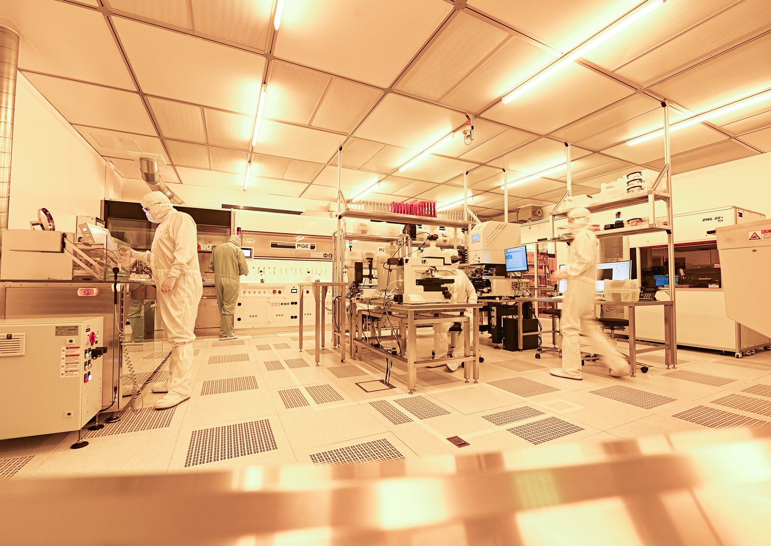
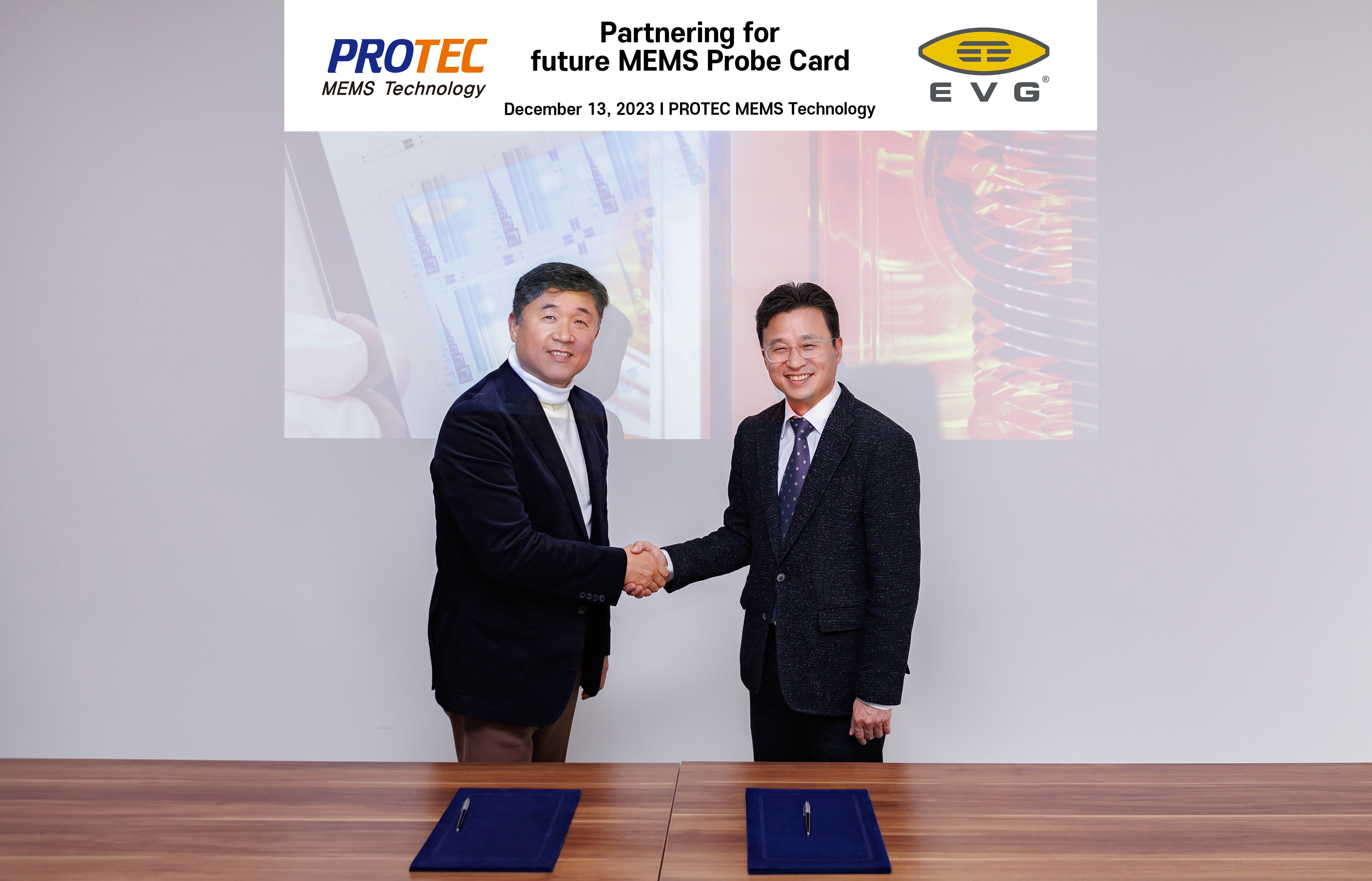
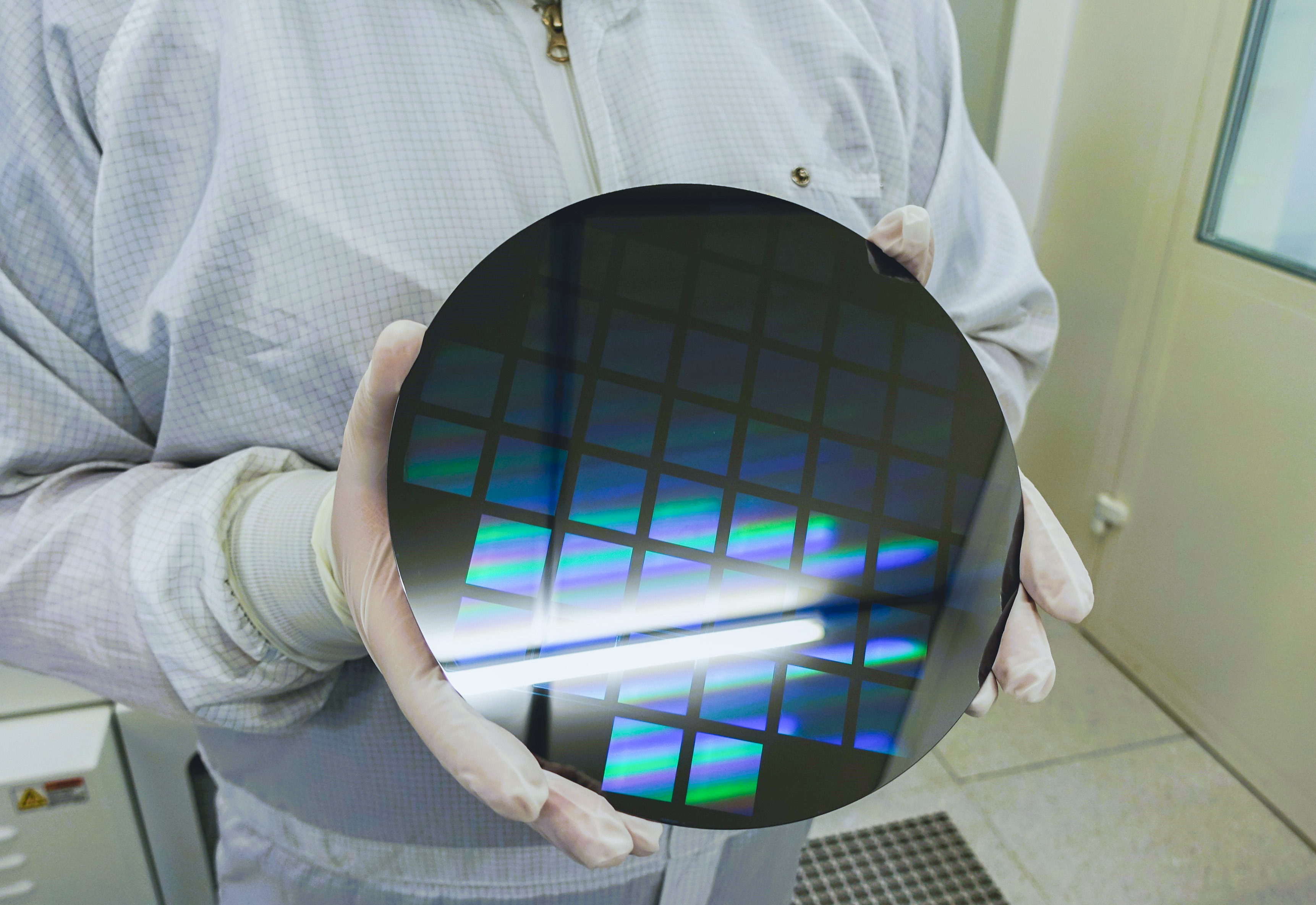
Protec MEMS Technology Orders Maskless Lithography System from EV Group for Advanced Memory Wafer Probe Card Manufacturing
07.12.2023
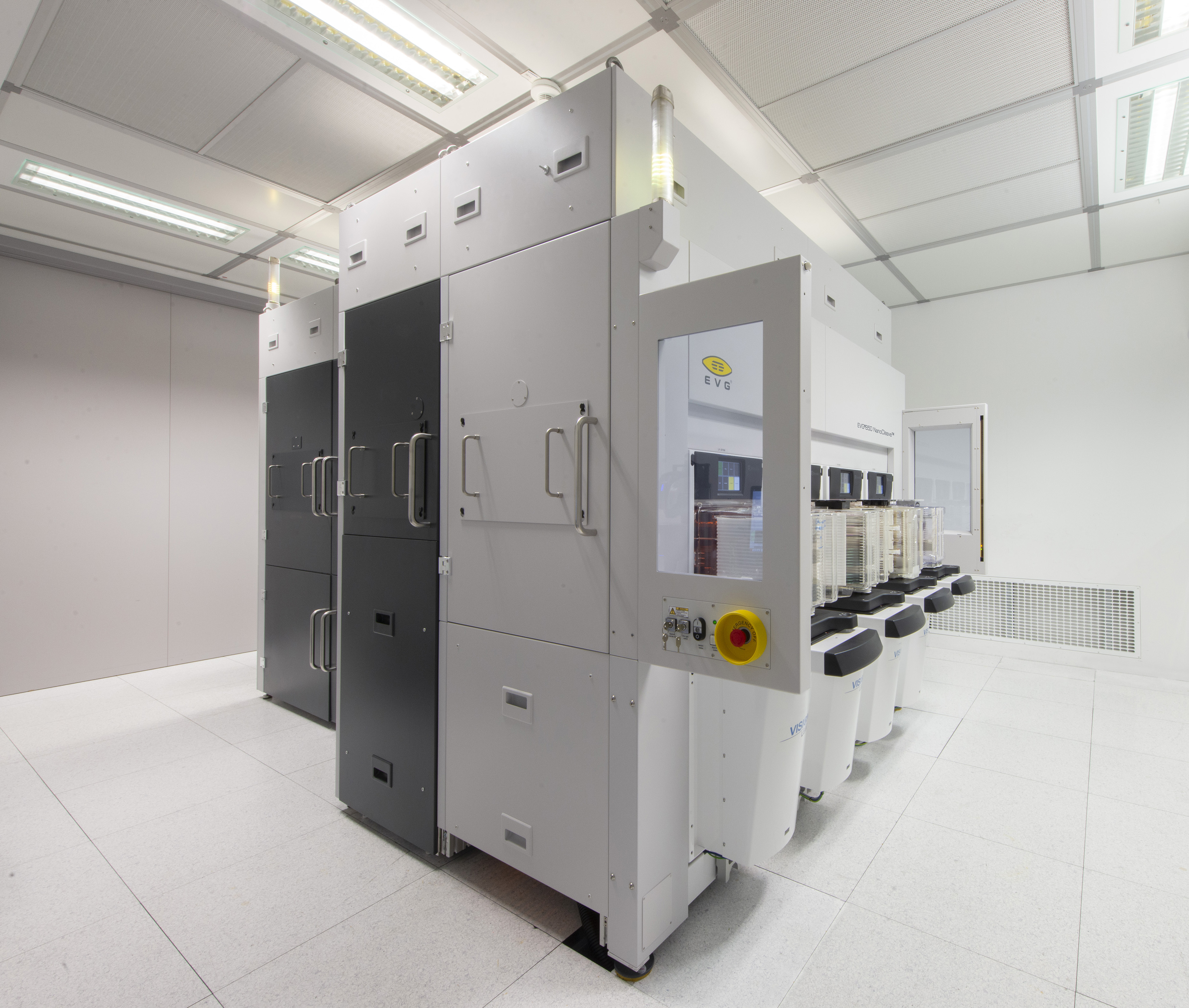
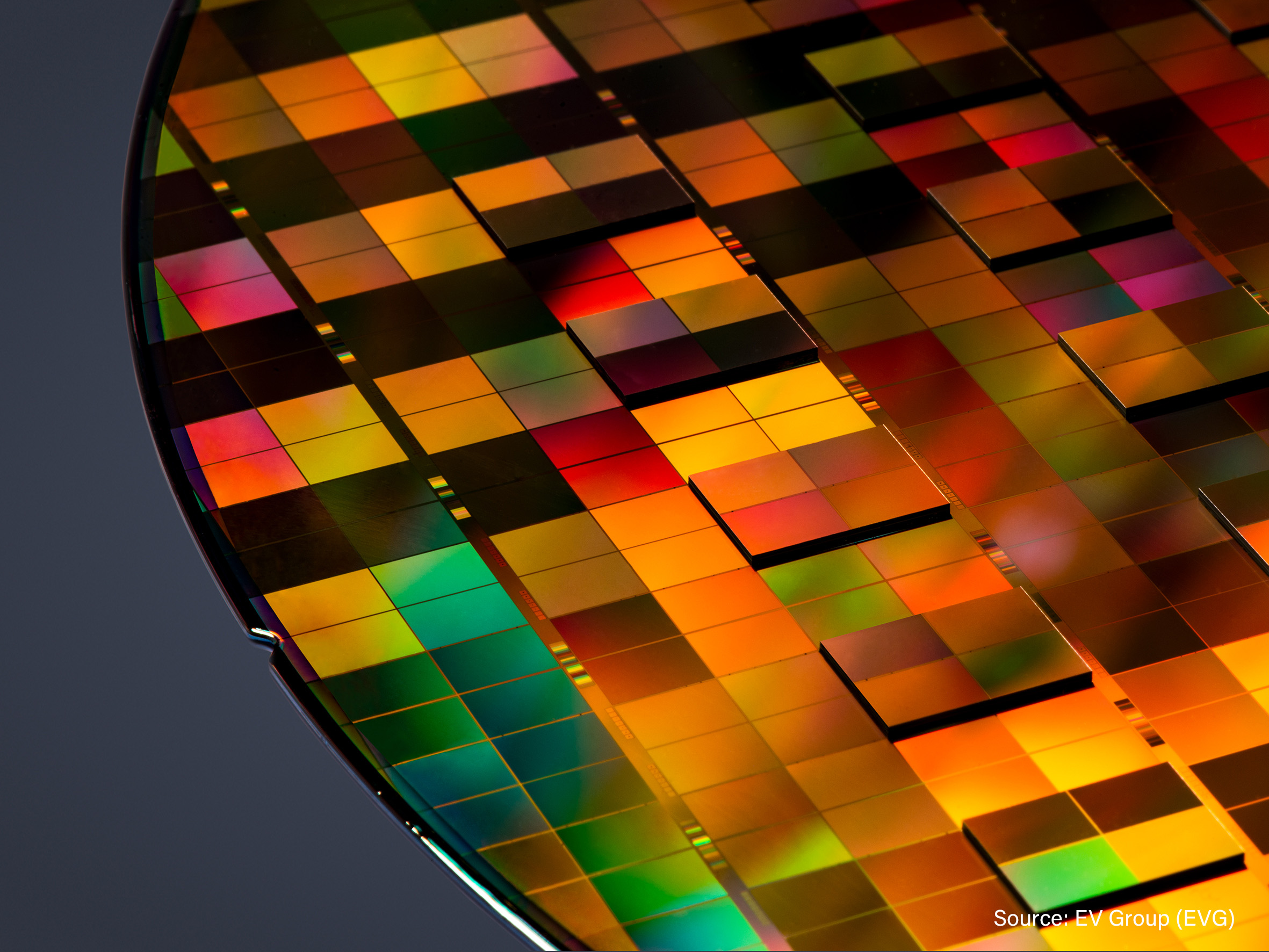
EV Group Brings Revolutionary Layer Transfer Technology to High-Volume Manufacturing with EVG®850 NanoCleave™ System
28.11.2023
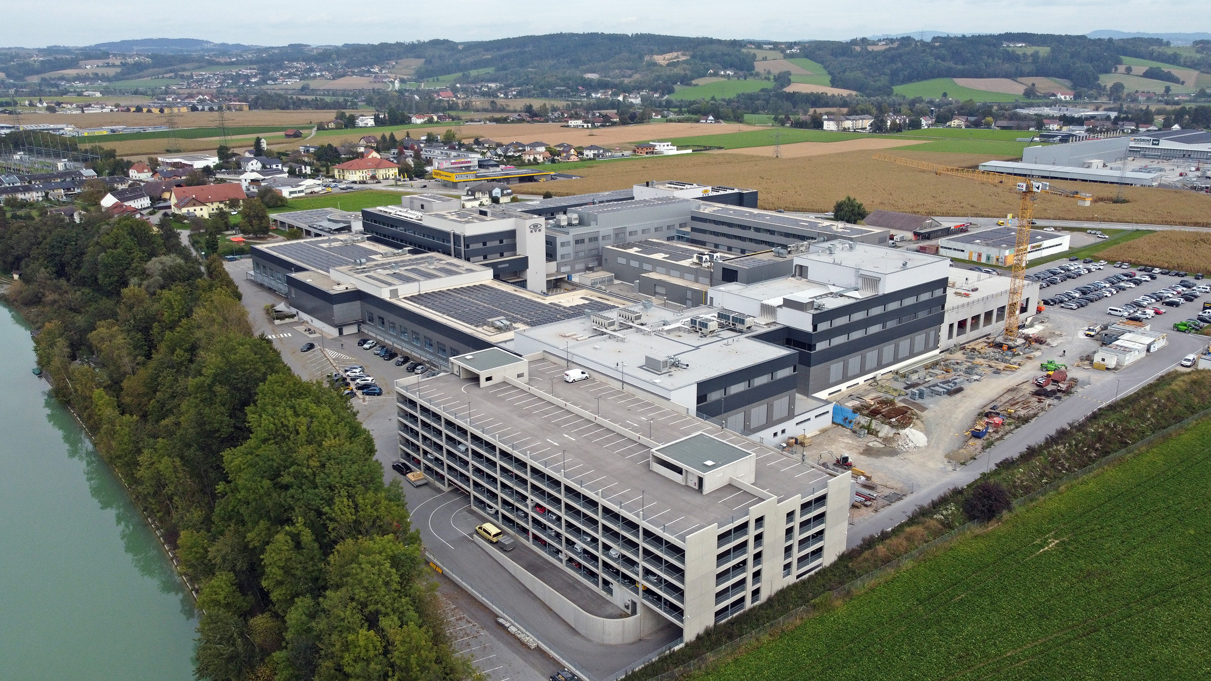
EV Group Completes Construction of New Manufacturing V Building at Corporate Headquarters to Expand Production Capacity
13.11.2023
Silicon Austria Labs and EV Group strengthen Collaboration in Optical Technology Research
25.10.2023
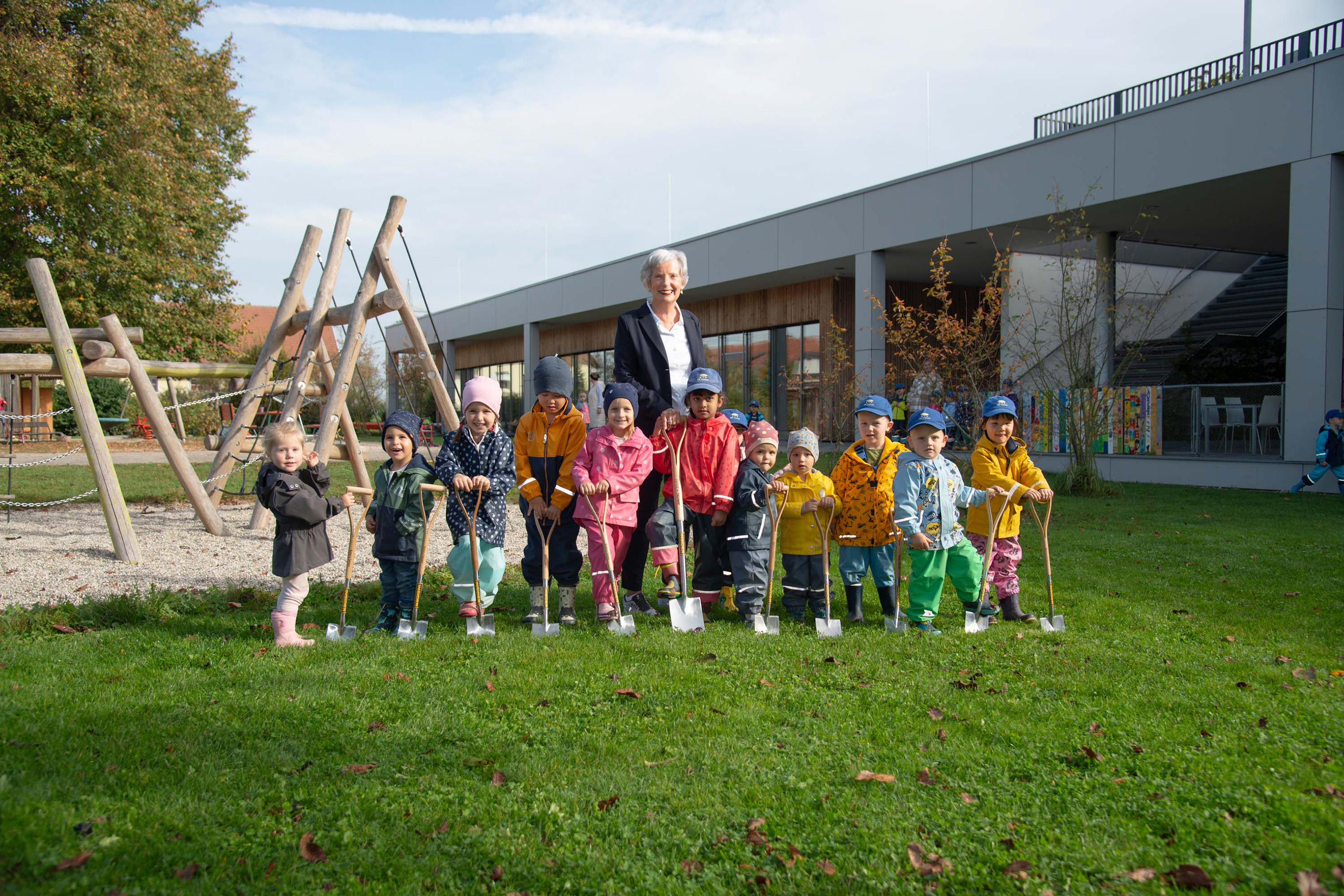
10 Years of EVG Minis: Lighthouse Project for Family-friendly Workplace Celebrates Milestone Birthday - And Continues Growth
28.08.2023
EV Group Hybrid Bonding and Nanoimprint Lithography Solutions to be Highlighted at SEMICON Taiwan 2023
27.06.2023