事件
ICEP 2024
Listen to our talks "Synchronization of Process and Material to Achieve Best Results in NanoImprinting Lithography" held by our Senior Process Enigeer Schuster Patrick and "Advanced Manufacturing Techniques for Freeform Micro-Optics Elements" held by our Product Manager Dr. Dudus Anna on Friday 19th April in Room "A" at 2:00PM.
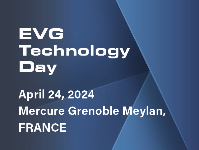
EVG NIL Technology Day 2024 in Grenoble
Wednesday, April 24, 2024
MicroNanoFabrication Annual Review Meeting 2024
Visit our booth at the MicroNanoFabrication Annual Review Meeting 2024!
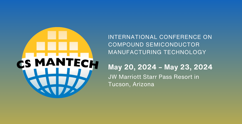
CS MANTECH 2024
Visit our booth #406!
ECTC 2024
Visit our booth #552 and our talk "Ultra–High Density RDL Patterning of High–Resolution Dielectrics by Maskless Exposure Technology for High Performance Computing and Artificial Intelligence Devices" held by Dr. Varga Ksenija!
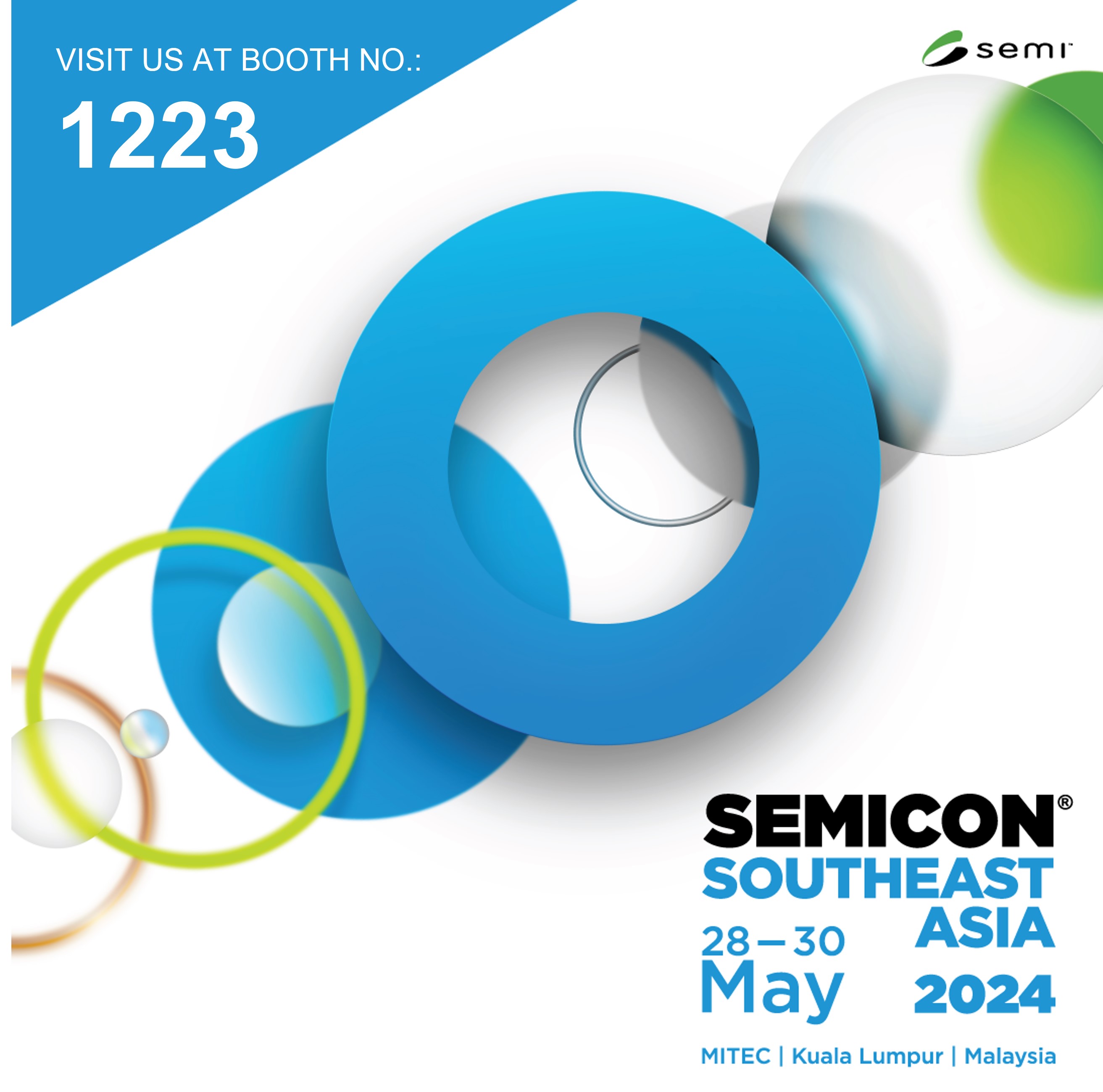
Semicon South East Asia 2024
Visit our booth #1223!
EMLC 2024
Be Part of the poster session starting on Tuesday June 18th, 17:30 and have a look on our
"Cost–effective Nanoscale Process Control Enabled by EVG‘s Metrology Systems" Poster.
& Listen to our talks on Wednesday June 19th,:
"Traceability in Automotive Enabled by Digital Lithography" held by Dr. Varga Ksenija in Session 10 and
"Utilizing Inkjet Coating and Nanoimprinting for Complex 3D Patterns with Gradual Height Increase and Minimal Residual Layer" held by Achleitner Thomas in Session 11.