仮接合・剥離
3次元積層のためのウェーハ裏面プロセスを可能にする仮接合・剥離技術
イントロダクション
仮接合は、3次元IC、パワーデバイスやファンアウト・ウェーハレベル・パッケージング(FoWLP)ウェーハなどの薄化済、または薄化されるウェーハ、さらに化合物半導体などの壊れやすい基板を機械的にサポートするために不可欠なプロセスです。EVGの仮接合装置は2001年に初リリースされ、EVGの蓄積されたウェーハ接合のノウハウのすべてが反映されています。
EVGでは、市販されている各種の材料に対応するオープンプラットフォームを採用し、仮接合や剥離のための完全なプロセス統合を提供しています。接着剤は主に、レーザー剥離、機械剥離、または熱剥離の手法(デバイスと支持基盤の間の接合を弱める各剥離手法)に基づき、分類されます。20年以上の経験を持つスライドオフとリフトオフ剥離は、EVGの仮接合技術の原点です。近年では、機械剥離とUVレーザーによる剥離を組み合わせたEVGのLowTemp剥離プロセス(室温での剥離)が開発されています。特に盛んに開発が行われているシリコンの裏面加工や次世代デバイス用の超薄型チップ・パッケージなどを可能にする低温剥離は先端パッケージング製造にとって不可欠な工程となっています。
特長
- 各種接着剤に対応したオープンプラットフォーム
- モジュール構成 - 顧客特有のプロセス用に装置を構成し、最適なスループットを提供
- 1台の設備で異なる基板サイズに対応可能
- 複数のロードポートオプションや組み合わせが可能
- 測定装置を自動装置内に搭載し、補正機能によるプロセスの高歩留まりを実現
- ソフトウェアによるすべてのプロセスパラメータをリアルタイムにモニタリング
- SECS/GEMインターフェイスを搭載
数値


Events
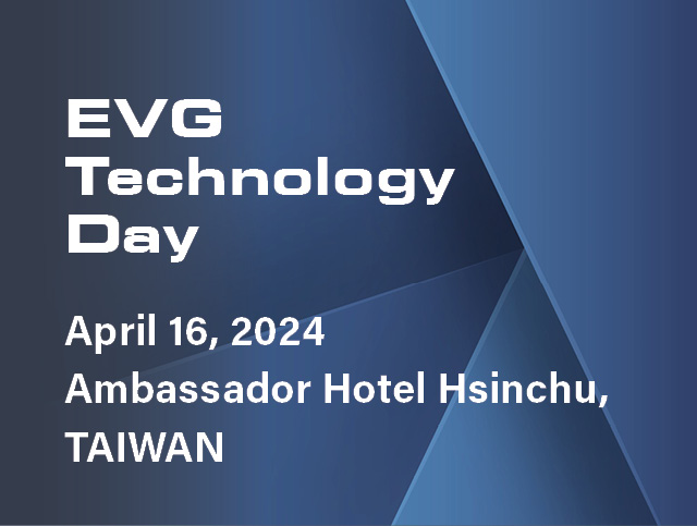
EVG Technology Day 2024 in Taiwan
Register now for the EVG Technology Day in Taiwan at the Hsinchu Ambassador Hotel on April 16 ,2024!
CS / PIC / PE International Conference 2024
Visit us at our booth at the CS / PIC and PE International Conference and listen to our talks:
"Heterogenous Integration of Compound Semiconductors by W2W and D2W Bonding" held by Business Development Manager Bernd Dielacher at the CS Conference.
"Advances in PIC Manufacturing for Sensing and Datacom Applications – All Thanks to Nanoimprint Lithography" held by Business Development Manager Jonas Khan at the PIC Conference.
"Cost-effective SiC substrate manufacturing for power devices enabled by oxide-free wafer bonding" held by Business Development Manager Bernd Dielacher at the PE Conference.
ICEP 2024
Listen to our talks "Synchronization of Process and Material to Achieve Best Results in NanoImprinting Lithography" held by our Senior Process Enigeer Schuster Patrick and "Advanced Manufacturing Techniques for Freeform Micro-Optics Elements" held by our Product Manager Dr. Dudus Anna on Friday 19th April in Room "A" at 2:00PM.

Talk to our EVG technology experts!
Questions?
Related products
Questions about our technologies?
Contact the EVG experts