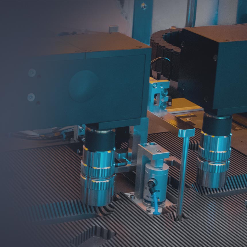
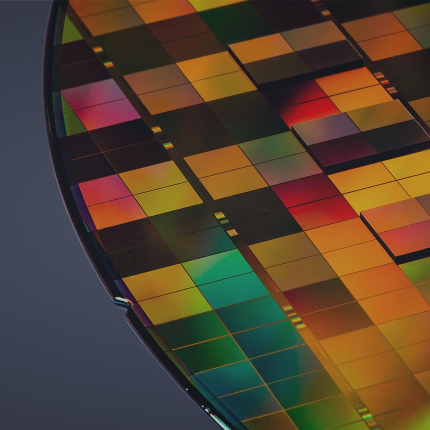
Technologies
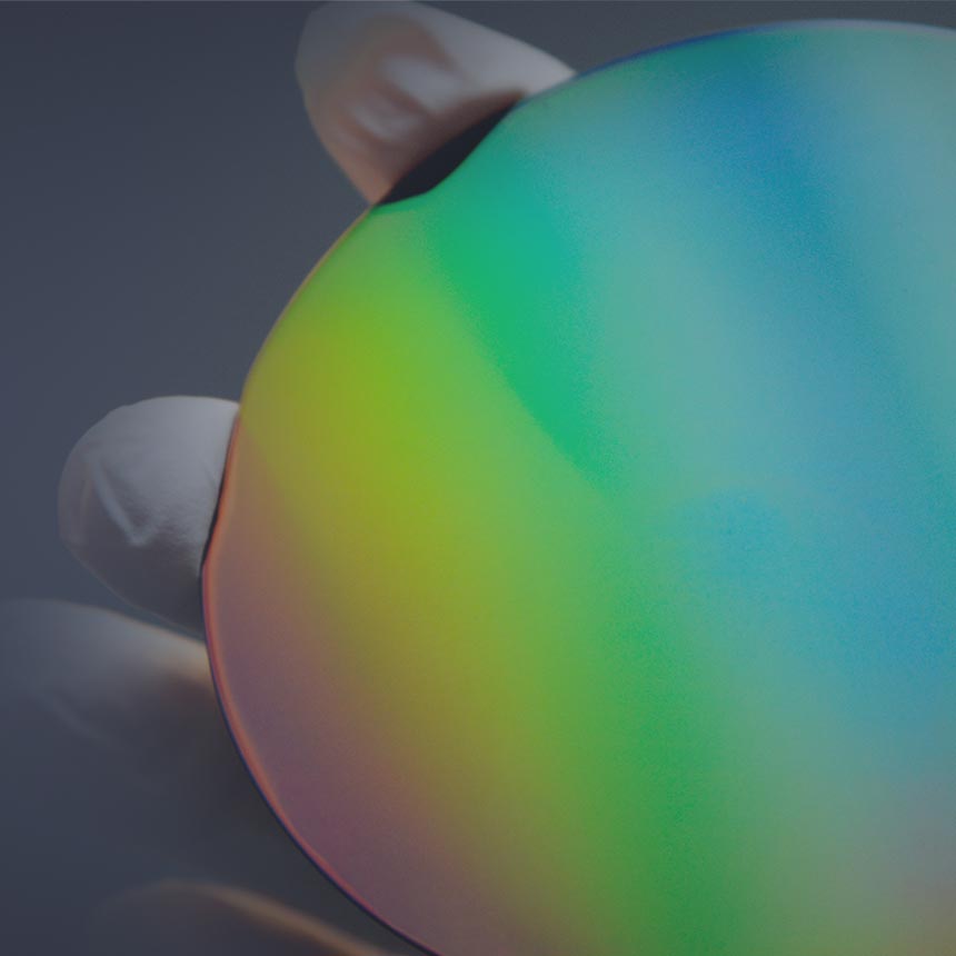
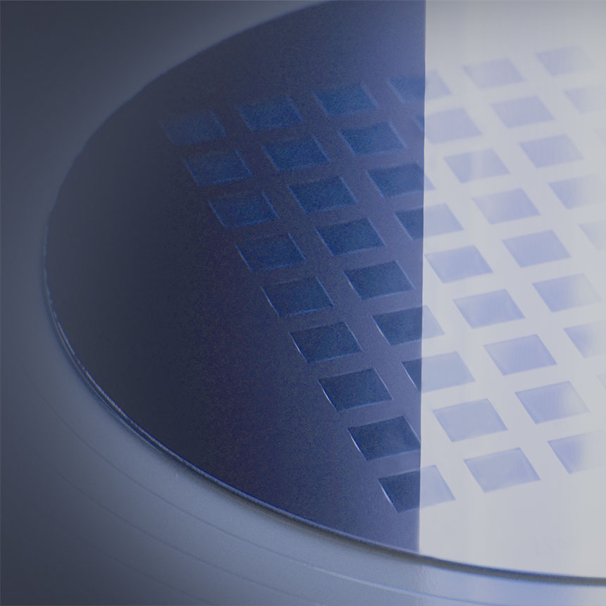
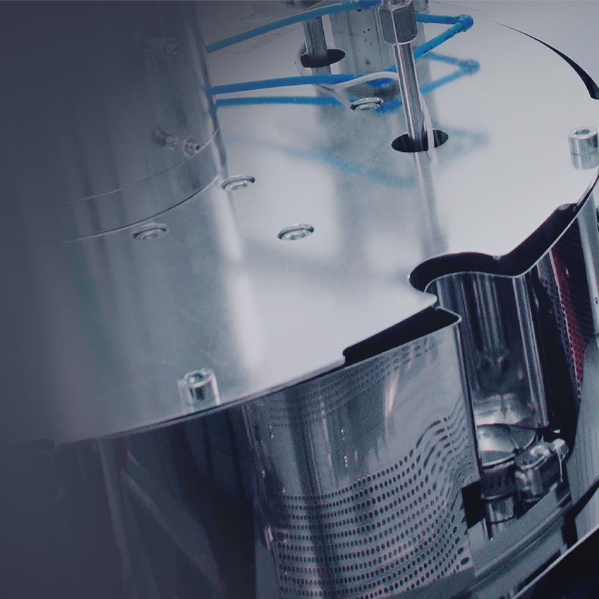
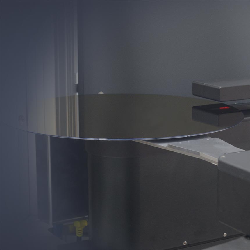
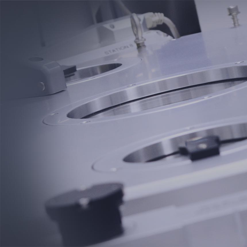
For nearly 40 years, EVG has provided industry-leading process technologies and solutions that have enabled innovations in advanced packaging, optics and photonics, sensors and bio-medical devices and applications.
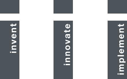
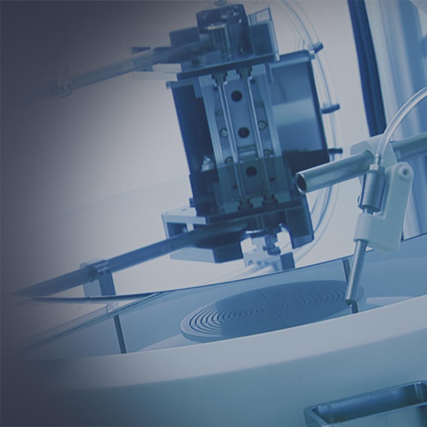
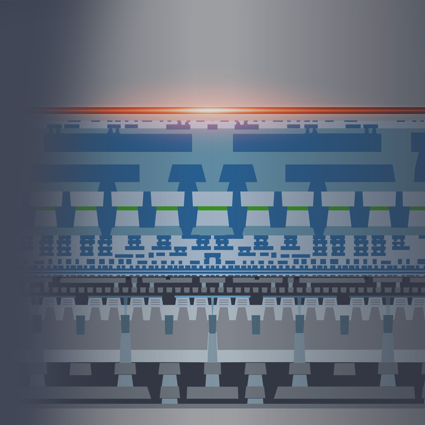
True to our Triple-i philosophy of “Invent”, “Innovate” and “Implement”, our core lithography, wafer bonding and metrology technologies enable manufacturers to develop the latest micro- and nanotechnology device breakthroughs, and then bring them into high-volume production, cost effectively and at high process yields.