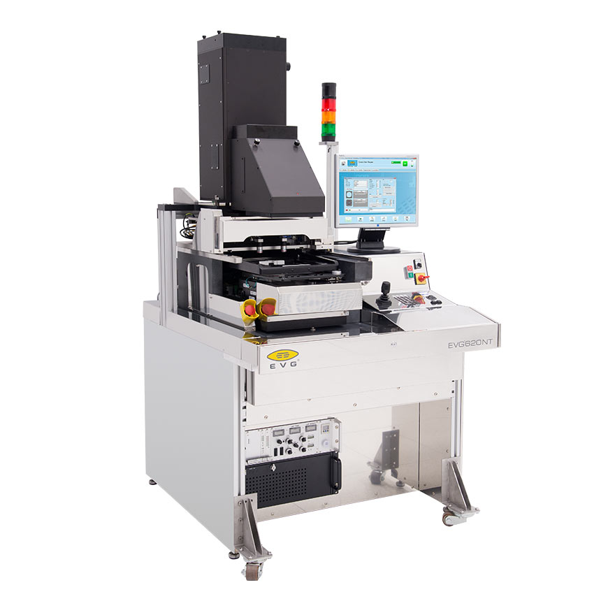
EVG®620 NT
Mask Alignment System
(semi-automated / automated)
The EVG®620 NT provides state-of-the art mask alignment technology on a minimized footprint area up to 150 mm wafer size.
Known for its versatility and reliability, the EVG620 NT provides state-of-the-art mask alignment technology on a minimized footprint area combined with advanced alignment features and optimized total cost of ownership. It is an ideal tool for optical double-side lithography available in semi-automated or automated configuration with optional full-housing Gen 2 solution to meet high-volume production requirements and fab standards. Operator-friendly software, minimized time for mask and tooling changes, as well as efficient worldwide service and support makes it the ideal solution for any manufacturing environment. The EVG620 NT or the fully housed EVG620 NT Gen2 mask alignment systems are equipped with integrated vibration isolation, and achieve excellent exposure results for a wide range of applications, such as exposure of thin and thick resists, patterning of deep cavities and comparable topographies, as well as processing of thin and fragile materials such as compound semiconductors. Furthermore, the EVG’s proprietary SmartNIL technology is supported on both semi-automated and fully automated system configurations.
Features
- Wafer/substrate size from pieces up to 150 mm/6’’
- System design supporting versatility of lithography processes
- Fragile, thin or warped wafer handling of multiple wafer sizes with quick change-over time
- Automated contact-free wedge compensation sequence with proximity spacers
- Auto origin function for precise centering of alignment key
- Dynamic alignment function featuring real-time offset correction
- Supports the latest UV-LED technology
- Rework sorting wafer management & flexible cassette system
- Manual substrate loading capability on automated system
- Field upgradeable from semi-automated to fully automated version
- Minimized system footprint and facility requirements
- Multi-user concept (unlimited number of user accounts and recipes, assignable access rights, different user interface languages)
- Advanced SW features and compatibility between R&D and full-scale production
- Agile processing and conversion re-tooling
- Remote tech support and SECS/GEM compatibility
- Additional capabilities:
- Bond alignment
- IR alignment
- Nanoimprint lithography (NIL)

Technical Data
| Exposure source |
|---|
| Mercury light source / UV LED light source |
| Advanced alignment features |
|---|
| Manual alignment / in-situ alignment verification |
| Automatic alignment |
| Dynamic alignment / automatic edge alignment |
| Alignment offset correction algorithms |
| Throughput |
|---|
| Fully-automated: throughput first print: 180 wafers per hour |
| Fully-automated: throughput aligned: 140 wafers per hour |
| Wafer diameter (substrate size) |
|---|
| Up to 150 mm |
| Alignment modes |
|---|
| Top side alignment: ≤ ± 0,5 µm |
| Bottom side alignment: ≤ ± 1,0 µm |
| IR alignment: ≤ ± 2,0 µm/ substrate material depending |
| Bond alignment: ≤ ± 2,0 µm |
| NIL alignment: ≤ ± 3,0 µm |
| Exposure setup |
|---|
| Vacuum contact / hard contact / soft contact / proximity mode / flex mode |
| Wedge compensation |
|---|
| Fully automatic - SW controlled |
| Exposure options |
|---|
| Interval exposure / flood exposure / sector exposure |
| System control |
|---|
| Operations system: Windows |
| File sharing & back-up solution / unlimited no. recipes & parameters |
| Multi-language user GUI & support: CN, DE, FR, IT, JP, KR |
| Real-time remote access, diagnostics & troubleshooting |
| Industrial automation features |
|---|
| Cassette / SMIF / FOUP / SECS/GEM / thin, bowed, warped, edge wafer handling |
| Nanoimprint lithography technology |
|---|
| SmartNIL® |

Talk to our EVG product experts!
Questions?
Related technologies
Questions about our products and technologies?
Contact the EVG experts