Temporary Bonding Systems
Temporary bonding is an essential process to offer mechanical support for thin or to-be-thinned wafers, important for 3D ICs, power devices and FoWLP wafers, as well as for handling fragile substrates like compound semiconductors. A device wafer is bonded to a carrier wafer with the help of an intermediate temporary bonding adhesive, allowing the typically fragile device wafer to be processed with additional mechanical support. After the critical processes, the wafer stack is debonded. EVG’s outstanding bonding know-how is reflected in its temporary bonding equipment, which has been provided by the company since 2001.
Choose your Temporary Bonding System

EVG®805
Debonding System
Thin wafer debonding.

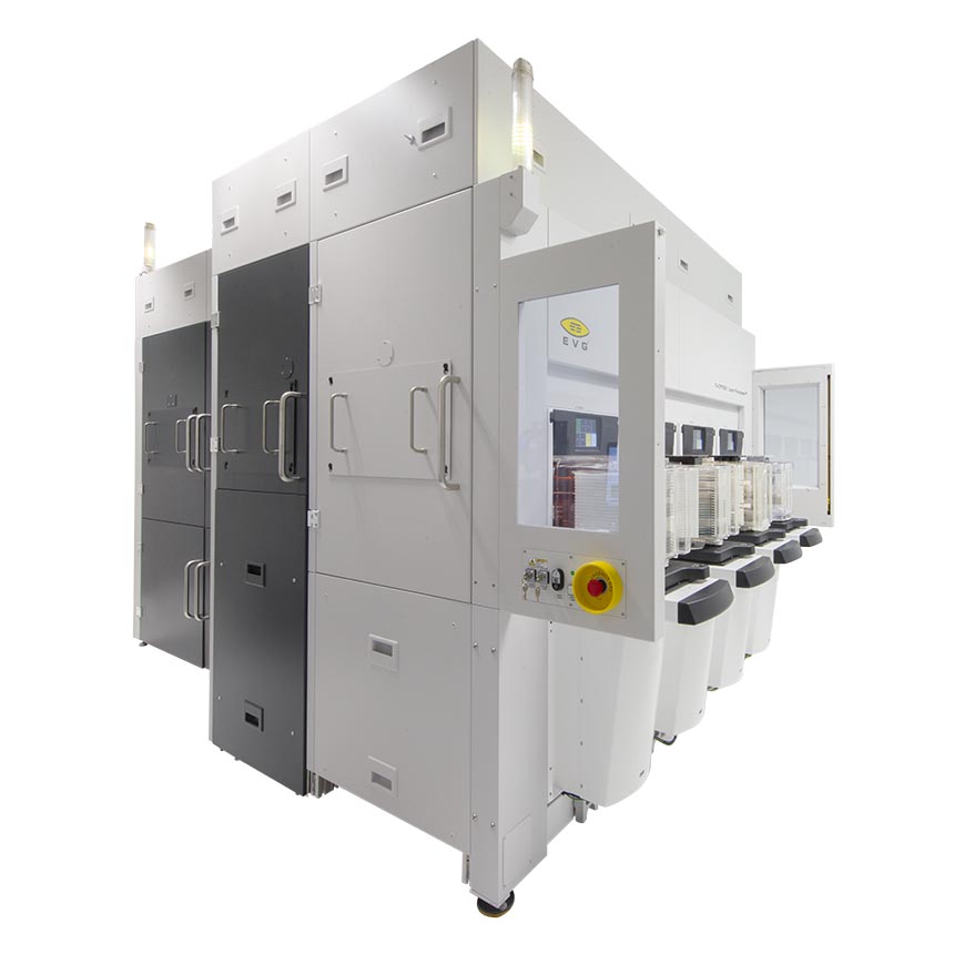
EVG®850 TB
Automated Temporary Bonding System
Fully automated temporary wafer bonding of a substrate on a rigid carrier.

EVG®850 DB
Automated Debonding System
Fully automated debonding, cleaning and unloading of thin wafers.
EVG®880 LayerRelease™
Automated Layer Release System
The EVG®880 LayerRelease™ System is a fully automated system and enables precise release of layers from silicon carrier substrates using an IR laser.

Talk to our EVG product experts!
Questions?
Questions about our products and technologies?
Contact the EVG experts
Download
EVG® Solutions for Temporary Bonding and Debonding Brochure