About EVG
Short Profile
EV Group (EVG) is a leading supplier of high-volume production equipment and process solutions for the manufacture of semiconductors, MEMS, compound semiconductors, power devices and nanotechnology devices.
A recognized market and technology leader in wafer-level bonding and lithography for advanced packaging and nanotechnology, EVG’s key products include wafer bonding, thin-wafer processing and lithography/nanoimprint lithography (NIL) equipment, photoresist coaters, as well as cleaning and inspection/metrology systems.
With state-of-the-art application labs and cleanrooms at its headquarters in Austria, as well as in North America and Asia, EVG is focused on delivering superior process expertise to its global R&D and production customer and partner base – from the initial development through to the final integration at the customer’s site.
Founded in 1980, EVG services and supports an elaborate network of global customers and partners all over the world, with more than 1300 employees worldwide and fully-owned subsidiaries in the U.S., Japan, South Korea, China and Taiwan.
Vision/Mission
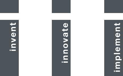
invent – innovate – implement
Our Triple-i philosophy is reflected in the enthusiasm for technology, innovative strength and internationality of the entire company. Our vison of “being the first in exploring new techniques and serving next-generation applications of micro- and nanofabrication technologies” enables our customers to successfully commercialize their new product ideas.
Our Story
Impact
Aided by our manufacturing technology, all kinds of microchips as well as other electronic, micro-mechanical and optical components with microscopically small structures are created on thin discs, known as “wafers”, or other substrates, which are made of silicon, glass or similar materials.
At the manufacturing sites of our global customers, EVG’s precision mechanical engineering systems are used to produce key components such as camera sensor chips, position- and motion-sensors, microphones and displays for smartphones, virtual reality glasses and gaming consoles. In addition, our technology enables airbag sensors and central components for advanced driver assistance systems in modern cars, as well as pioneering bio-medical products such as micro-fluidic chips that facilitate blood analysis on-site at a medical office or lab, or DNA analysis for early detection screening.
History
Since our founding by DI Erich and Aya Maria Thallner in 1980, a mix of bold, innovative thinking and a commitment to developing leading-edge, quality manufacturing systems has paved the way for EVG’s global success as a leading supplier of equipment and process solutions for the semiconductor industry and related markets.
EVG continues to shape the industry, working with nearly every major semiconductor and MEMS manufacturer today. We developed the world’s first double-side mask aligner with bottom-side microscopes, which enabled the widespread commercialization of MEMS products, in 1985. The process separation between wafer alignment and wafer bonding, developed in 1990, revolutionized wafer bonding technology and has since become an industry standard. The first production wafer bonding system for volume MEMS manufacturing, introduced in 1992, laid the foundation for EVG’s market leadership in wafer bonding systems. Subsequent innovations included the patented SmartView® face-to-face wafer alignment technology for wafer-level packaging and 3D interconnect introduced in 1999, the industry’s first integrated production wafer bonding system launched under the name GEMINI® in 2000, temporary wafer bonding and debonding technology (developed as early as 2001) and the world's first fully automated production wafer bonding system for 300 mm wafers launched in 2007. The groundbreaking ComBond® high-vacuum cluster tool, introduced in October 2014, enabled electrically conductive and oxide-free covalent bonds at room temperature for engineered substrate and power device production applications and paved the way for completely new and innovative MEMS developments. With the HERCULES® NIL, launched in July 2015, EVG ramped nanoimprint lithography (NIL) into high-volume manufacturing. In December 2018, EVG unveiled BONDSCALETM, the company’s next-generation fusion wafer bonder for "More Moore" scaling and front-end processing to address future logic transistor scaling and 3D integration challenges outlined in the IRDS Roadmap. In September 2020, EVG introduced the first LITHOSCALE® systems, incorporating EVG’s new MLE™ (Maskless Exposure) technology to bring the benefits of digital lithography in high-volume manufacturing to a wide range of applications and markets.
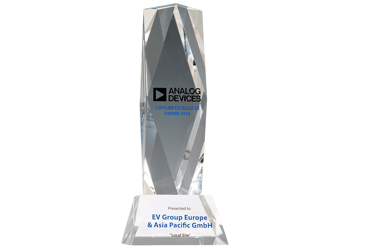
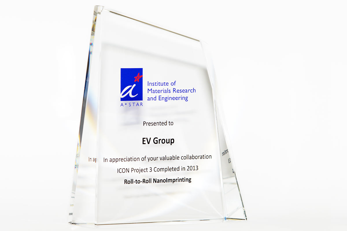
Awards and Recognitions
A selection


 in the “industry” category by Austria’s BezirksRundschau magazine")


Corporate Social Responsibility
EV Group (EVG) is a responsible global organization committed to safeguarding the welfare of our society and the environment in which we work.
In order to conduct all operations in an environmentally and socially responsible manner, and create environmentally and socially friendly practices, EVG operates an Environmental Management System according to ISO 14001 standard. Through careful handling of resources and energy, and by reducing solid waste, emissions and wastewater, EVG continuously improves its environmental performance.
As part of EVG’s corporate social responsibility, EVG complies with and also demands that all suppliers comply with applicable legal requirements and regulations regarding occupational health and safety, equality, accident prevention, equipment safety, environmental protection, as well as anti-bribery and corruption. EVG has committed itself to the Responsible Business Alliance (RBA) Code of Conduct (formerly known as “EICC Code of Conduct”), supports the 2010 Dodd-Frank Act (“Conflict Minerals”), and is dedicated to prohibiting the receipt of goods and/or services from suppliers known to have violated occupational health and safety provisions and - in particular - human rights, including child labor, slavery, or forced labor to name a few examples.
EVG ensures equality to all employees, irrespective of age, cultural background, class, disability, ethnicity, gender, sexual orientation, faith and marital status. No form of discrimination, intimidation, bullying or harassment and no form of bribery, corruption and blackmailing is accepted by EVG. All employees, whether part time, full time or temporary, are treated fairly and equally, with dignity and respect, valuing the diversity of all. This policy applies to all aspects of employment from recruitment, training, and career development to promotion and redundancy. Selection for employment, promotion, training or any other benefit will be on the basis of aptitude and ability.
ISO 9001:2015
In 2002 EVG started implementing a QM-system according to "ISO 9001". The first certification was achieved in 2004. Since this time the certificate has been successfully extended or renewed by external audits on an annual basis.
The scope of the Quality Management System and the Environmental Management System covers the products and services of all EV Group organizations, which are located in St. Florian am Inn, Austria.