Nanoimprint Lithography (NIL) - SmartNIL®
A large-area soft UV-nanoimprint lithography process for high-volume manufacturing
Introduction
EVG is the market-leading equipment supplier for nanoimprint lithography (NIL). Pioneering this non-conventional lithography technique for many years, EVG mastered NIL and has implemented it in volume production on ever-increasing substrate sizes. EVG's proprietary SmartNIL technology is optimized by years of research, development and field experience to address nanopatterning requirements that cannot be supported by conventional lithography. SmartNIL provides superior conformal imprint results down to 40 nm.
NIL has proven to be the most cost-efficient way to enable nano-scale patterns on large areas since it is not limited by sophisticated optics that are required with optical lithography, and since it can provide optimal pattern fidelity for extremely small (sub-100 nm) structures.
EVG's SmartNIL is a full-field imprint technology based on UV exposure, providing a powerful next-generation lithography technique with almost unlimited structure size and geometry capabilities. Since SmartNIL incorporates multiple-use soft stamp processing, it also enables unmatched throughput with considerable cost-of-ownership advantages while preserving scalability and maintenance-friendly operation. In addition, the lifetime of the master template is extended to periods comparable to masks used for optical lithography.
New application developments are often closely linked to advances in equipment capabilities. SmartNIL is a key enabling technology for many new innovations in displays, biotechnology and photonic applications. For example, SmartNIL provides unmatched full-area conformal imprinting in order to fulfill the most important criteria for wire grid polarizers on panel substrates. SmartNIL is also ideally suited for high-precision patterning of microfluidic chips with complex nanostructures to support the production of next-generation pharmaceutical research and medical diagnostics devices. Furthermore, recent developments in SmartNIL offer additional degrees of freedom to manufacture innovative photonic structures with the highest functionality, smallest form factors and high volumes, which are key for enabling Diffractive Optical Elements (DOEs), optical waveguides and other micro- and nanophotonic elements used for 3D sensing and biometric authentication.
Features
- Volume-proven imprinting technology with superior replication fidelity
- Proprietary SmartNIL® technology with multiple-use polymer stamp technology
- Production-proven resolution down to ≤ 40 nm
- Large-area full-field imprinting
- Lowest total cost of ownership
- Imprinting over topographies
- Alignment capability
- Room-temperature process
- Open materials platform
Figures


. Courtesy of Fraunhofer ISE")
Events
ICEP 2024
Listen to our talks "Synchronization of Process and Material to Achieve Best Results in NanoImprinting Lithography" held by our Senior Process Enigeer Schuster Patrick and "Advanced Manufacturing Techniques for Freeform Micro-Optics Elements" held by our Product Manager Dr. Dudus Anna on Friday 19th April in Room "A" at 2:00PM.
EVG NIL Technology Day 2024 in Grenoble
Wednesday, April 24, 2024
MicroNanoFabrication Annual Review Meeting 2024
Visit our booth at the MicroNanoFabrication Annual Review Meeting 2024!
Related downloads

Kontaktieren Sie unsere EVG-Technologieexperten!
Fragen?
Related products
Fragen zu unseren Technologien?
Kontaktieren Sie die EVG-Experten
Download Whitepaper
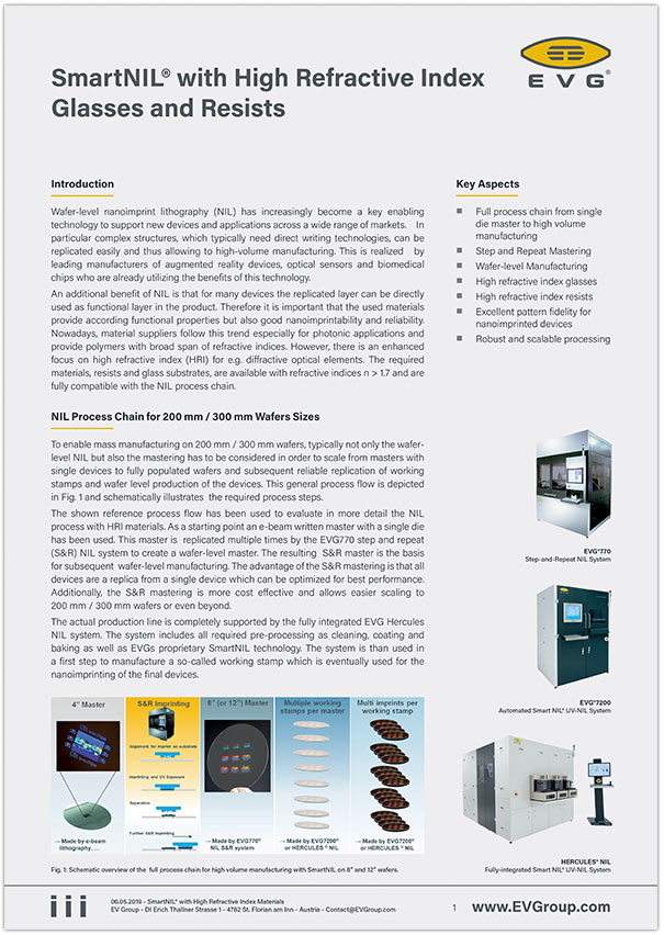
SmartNIL® with High Refractive Index Glasses and Resists