Technologien
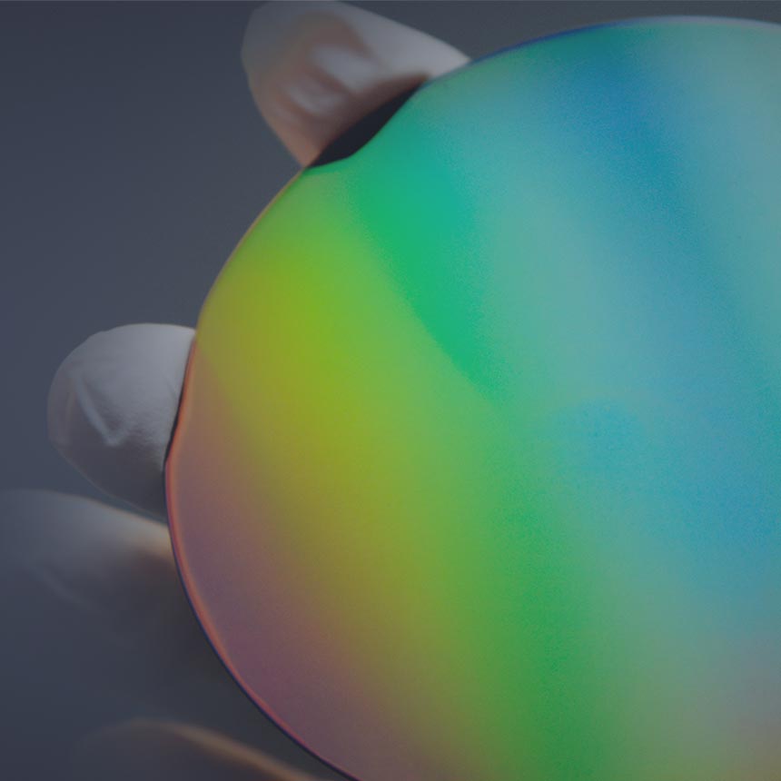
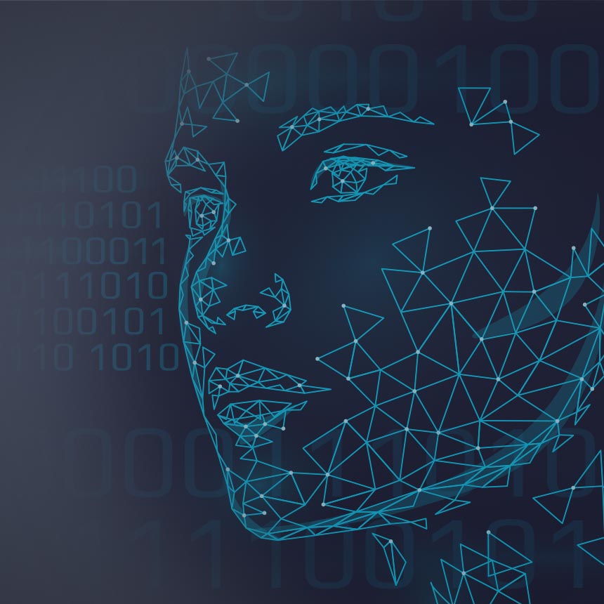
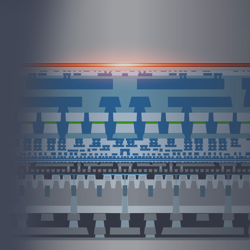
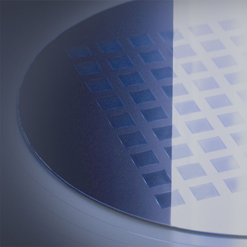
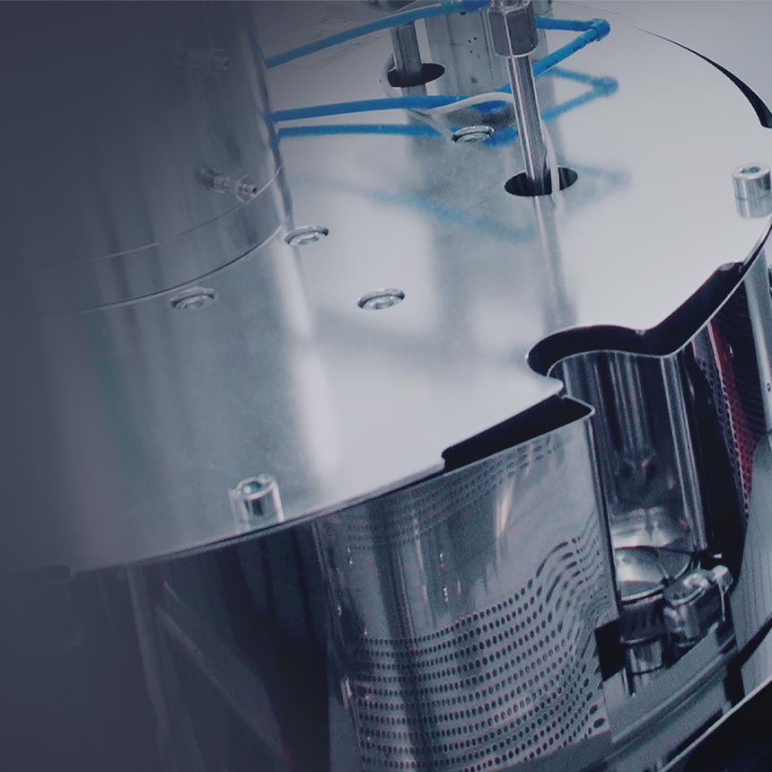
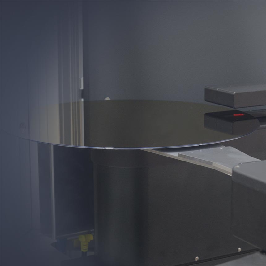
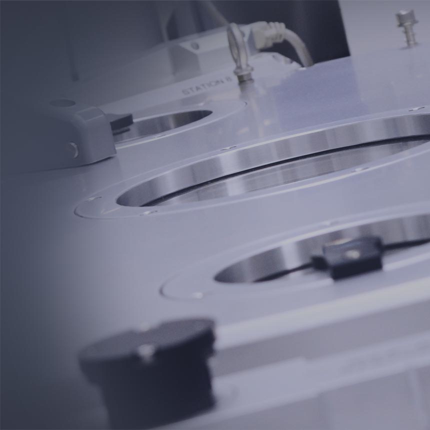
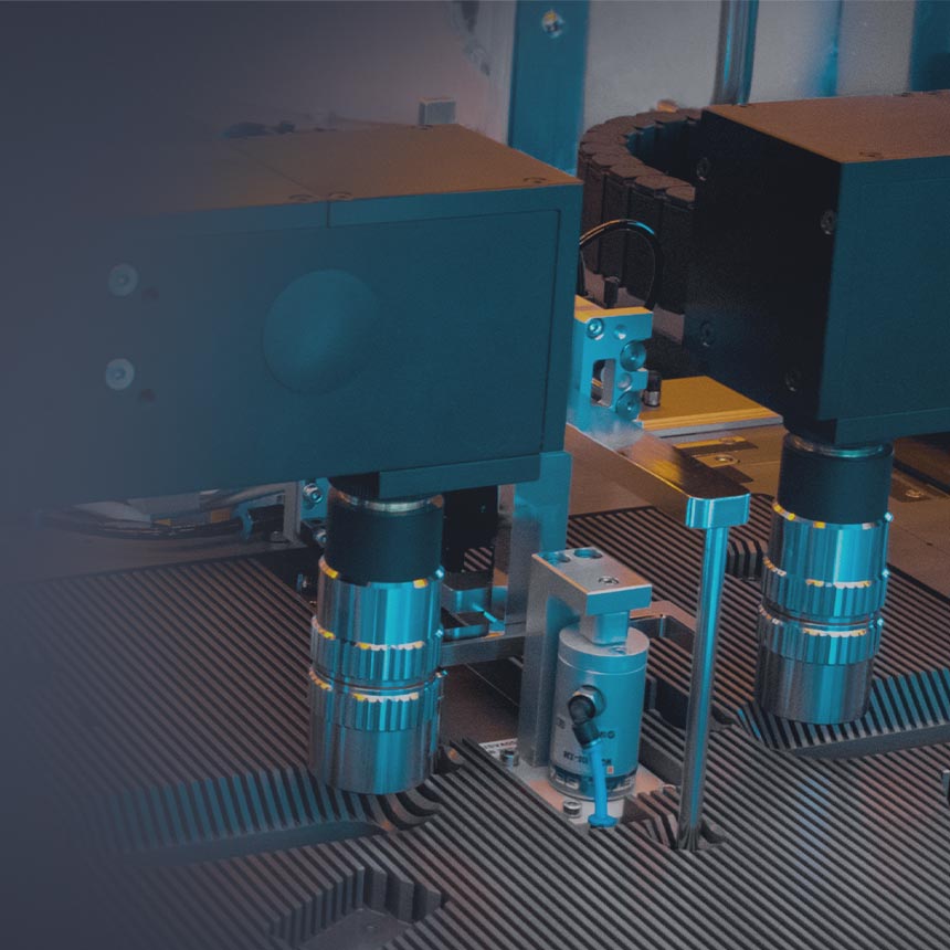
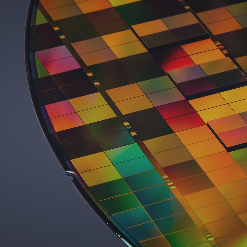
Die industrieweit führenden Prozesstechnologien von EVG ermöglichen seit fast 40 Jahren Innovationen bei Produkten und Anwendungen in den Bereichen Advanced Packaging, Optik und Photonik, Sensorik sowie Bio- und Medizintechnik.
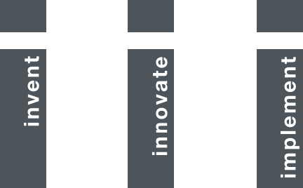
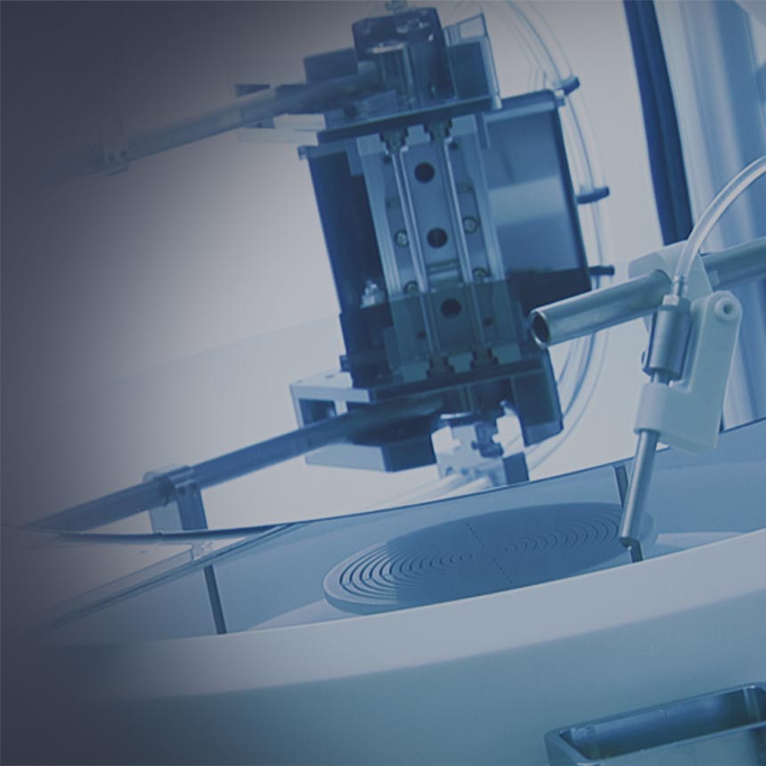
Getreu unserer Triple-i-Philosophie innovate – innovate – implement verhelften wir Herstellern durch unsere Kerntechnologien im Bereich Lithographie, Wafer-Bonding und Metrologie mit ihren neuesten Mikro- und Nanotechnologieprodukten zum Durchbruch. Wir unterstützen unsere Kunden bei der Umsetzung in die kosteneffektive Hochvolumenproduktion mit hoher Ausbeute.